Learn from the Quiz!
Thursday, 11 July 2019
12:00 AM
- There is a small resistance when looking into a voltage source
- You can model a voltage source in series with a resistor between any two terminals in a linear network
- In finding a Thevenin equivalent circuit, short circuit all independent voltage sources
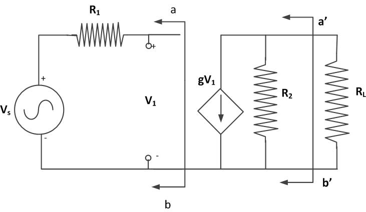
- The Norton
current between and is

- The Thevenin
resistance between and is

- The Thevenin
voltage between and is

- The value of should be much larger than for maximum voltage transfer to the load

- If a certain two
port network has as one of its admittance paramaters, should be

- The 3 dB frequency
- Is where the gain is reduced by approximately 70%
- Is where power is reduced by half
- Is where power is reduced by 3 dB
- For a transfer function which has two poles at 500 & 200000, and two zeros at 10000 & 15000, the pole at 500
- Will reduce the magnitude of the gain by 20 dB per decade from 500 onwards
- Will introduce a phase shift of 45 degrees at 500
- Will introduce a phase shift of 49 degrees at 5000
- For a transfer
function , the gain
magnitude at is approximately

- For a transfer
function , the bandwidth is

- With an (ideal) op-amp
- The inverting and non-inverting inputs are at virtual ground
- No current flows into the input of the op-amp
- It is direct coupled
- Very large open-loop gain
- Infinite bandwidth
- Very large input resistance
- The compensation capacitor provides the op-amp stability by creating a dominant pole
- Suppose the unity
gain frequency of a particular op-amp with an internal compensation
capacitor is .

- When configured
as a non-inverting amplifier with a gain of 100, the bandwidth would be

- When configured
as an inverting amplifier with a gain of -100, the bandwidth would be

- Suppose the unity
gain frequency of a particular op-amp with an internal compensation
capacitance of is . The unity gain
frequency would change to be larger than if the compensation capacitor were to be
changed to

- DC imperfections result in
- Input offset voltage
- Input offset current
- Input bias currents
- Output offset voltage DC imperfections in non-ideal op-amps are caused by a mismatch in input transistors
-------
- Electrons in the conduction band and valence band are responsible for current conduction in silicon
- By convention, the direction of current is assumed positive in the direction to which holes flow
- In intrinsic silicon
- The concentration of holes and electrons are dependent by temperature
- The concentration of holes and electrons are equal
- Hole movement is achieved by valence electrons hopping and filling holes
- To form n-type silicon, intrinsic silicon can be doped with phosphorus
- To form p-type silicon, intrinsic silicon can be doped with aluminium
- In doped silicon, the concentration of free carriers are controlled by the doping concentration
- In an extrinsic
semiconductor, if the doping concentration is

- The concentration
of majority carriers is approximately

- The concentration
of monitory carriers is inversely related to

- Current flow in semiconductors is achieved by
- Applying an electric field
- Concentration gradient in free carriers
- A n-type doped silicon is more conductive than a p-type doped silicon
- When an n-type doped silicon and p-type doped silicon is brought together and diffusion is possible across the contact area
- Holes diffuse from the p-type to the n-type piece
- Holes recombine with electrons in the n-type piece
- A depletion region is created across the PN junction with similar widths in each piece
- The potential barrier created within the depletion region
- Depends on temperature
- Depends on the majority carrier concentrations in the p-type and n-type
- The width of the depletion layer
- Gets narrower as the majority concentrations increase
- Gets wider when the PN junction is reverse biased
- Drift current does not increase when a PN junction is reverse biased
- Diffusion current reduces when a PN junction is reversed biased
- A forward biased PN junction results in a higher diffusion current
- In a forward biased PN junction, the forward current is caused by
- Holes injected from P to N
- Electrons injected from N to P
- Recombination of holes with electrons in the N type
- Recombination of electrons with holes in the P type
- The recombination of holes with electrons in the N type piece of a PN junction
- Contributes to the majority carrier forward current flow
- Decreases exponentially with distance from the edge of the depletion layer
- Is equal to the diffusion current of holes in the N type
- The forward current starts to increase exponentially once the knee voltage (of around 0.5-0.7V) is exceeded
- Zener diode breakdown occurs before avalanche breakdown
- The junction may break down if a large reverse voltage is applied
- For a BJT
- The base must be thin
- The Base-Emitter junction must be forward biased
- The Base-Collector junction must be reverse biased
- Doping concentration of the emitter is significantly higher than the base and collector
- BJTs usually operate in forward active mode
- For a BJT biased in forward active mode, the typical voltage between the base and emitter is around 0.7 V