DC Imperfections
Wednesday, 10 July 2019
7:29 PM
Consider an inverting amplifier where there is no input into either terminals
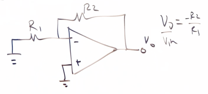
Ideally, would be zero, but this is not the case in
real life.![]()
There are DC imperfections within the op-amp which cause to be non-zero![]()
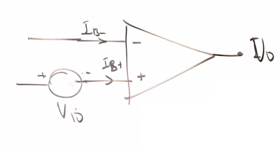
The transistors within the op-amp draw some current - known as the input bias current ( and )![]()
The mismatch of the transistors for the non-inverting and inverting
terminals cause ![]()
The input offset current ![]()
There is also an input offset voltage, where the non-inverting and inverting terminals have different potentials
BJT | Base-Emitter Voltage
MOSFET | Gate-Source voltage
Modelling the DC Imperfections
We need to consider the three causes of DC imperfection: input bias current, input offset current, and input offset voltage
We can calculate the maximum (worst case) output voltage offset with
![]()
![]()
So, then
![]()
![]()
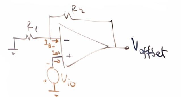
Apply superposition
To calculate , disable and and apply golden rules![]()
To calculate , disable and and apply golden rules![]()
To calculate , disable and and apply golden rules![]()