Assignment One
![Untitled picture.png Machine generated alternative text:
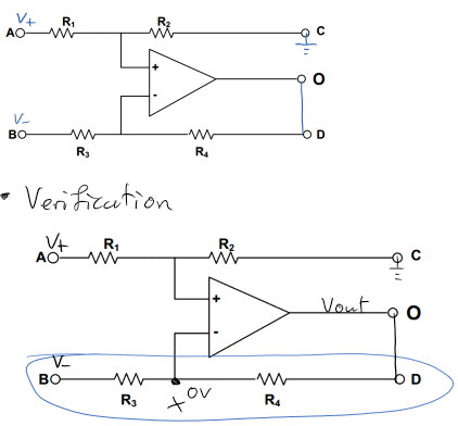
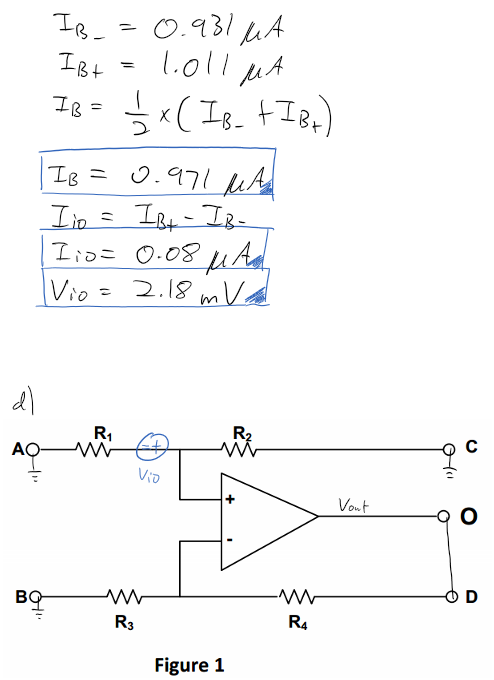
The circuit in figure l, with can be configured for a variety of
applications by the appropriate connection of terminals A, B, C, D, and O.
Untitled picture.png Figure 1
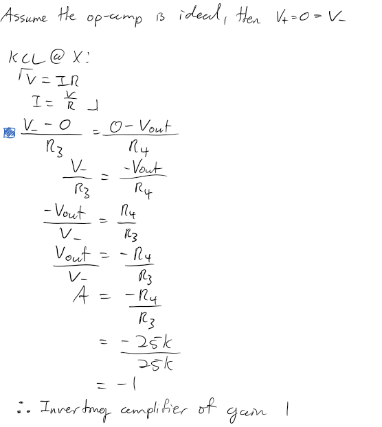
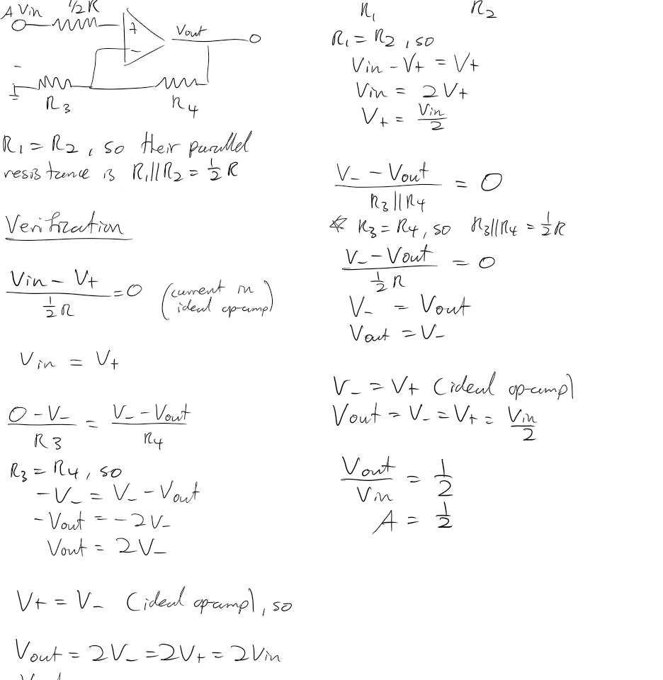
Untitled picture.png a) Show how the circuit can be used to implement a difference amplifier of unity gain.
[10 Marks]


](Assignment%20One_files/image001.png)
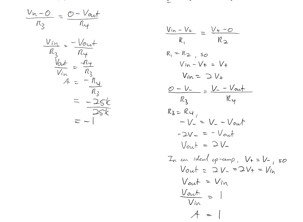
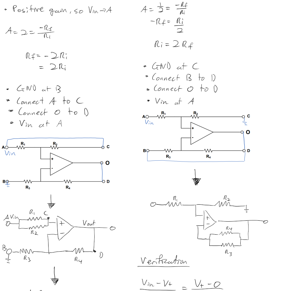
![Untitled picture.png b) Show how the circuit can be used to implement single-ended amplifiers with gains: (i)
-1; (ii) +1; (iii) +2; (W) +1/2.
In the implementation avoid from leaving a terminal open-circuited for such a terminal
may act as an "antenna" picking up interference and noise through capacitive coupling.
When more than one circuit implementation is possible, comment on the relative
merits of each from matching and input resistance point of
[20 marks]
Untitled picture.png Machine generated alternative text:
Untitled picture.png Machine generated alternative text:
Ink Drawings
Untitled picture.png Machine generated alternative text:
Ink Drawings
Untitled picture.png Machine generated alternative text:
Ink Drawings
Ink Drawings
Ink Drawings
Ink Drawings
Ink Drawings
Ink Drawings
Ink Drawings
Ink Drawings
Ink Drawings
Ink Drawings
Ink Drawings
Ink Drawings
Ink Drawings
Ink Drawings
Ink Drawings
Ink Drawings
Ink Drawings
Ink Drawings
Ink Drawings
Ink Drawings


Ink Drawings
Ink Drawings
Ink Drawings
Ink Drawings


Ink Drawings
Ink Drawings
Ink Drawings
Ink Drawings


](Assignment%20One_files/image004.png)


|
|
|||||||||||||||||
|
|
|||||||||||||||||
|
|
|||||||||||||||||
|
|
|||||||||||||||||
|
|
|||||||||||||||||
|
|
|||||||||||||||||
|
|
|||||||||||||||||
|
|
|||||||||||||||||
|
|
|||||||||||||||||
|
|
|||||||||||||||||
|
|
|||||||||||||||||
|
|
|||||||||||||||||
|
|
|||||||||||||||||
|
|
|||||||||||||||||
|
|
|||||||||||||||||
|
|
|||||||||||||||||
|
|

|
|
|||
|
|
 |
||
|
|
 |
||
|
|
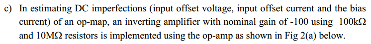
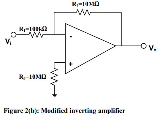
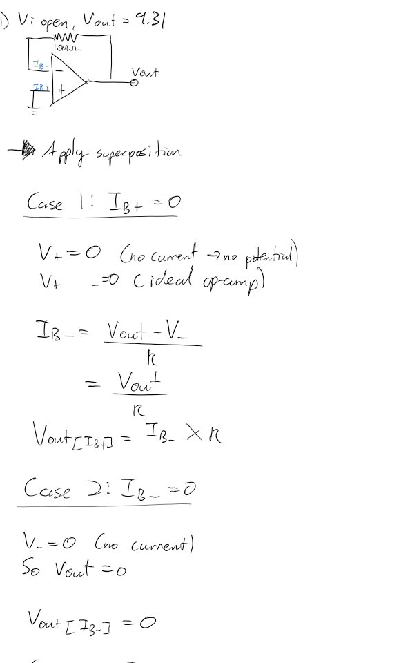
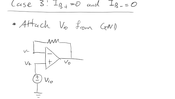
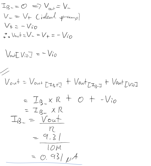
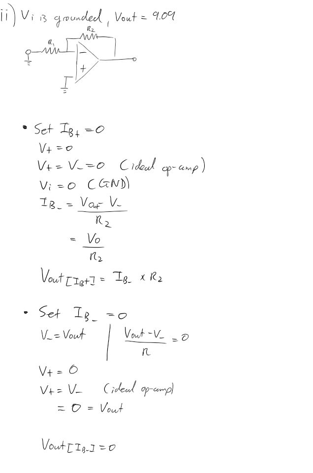
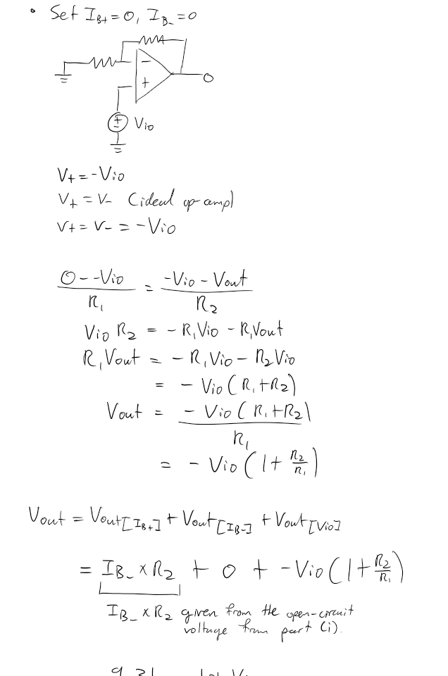
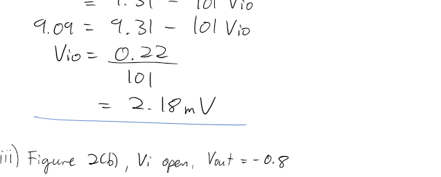
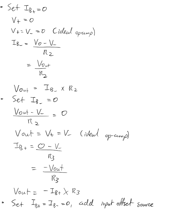
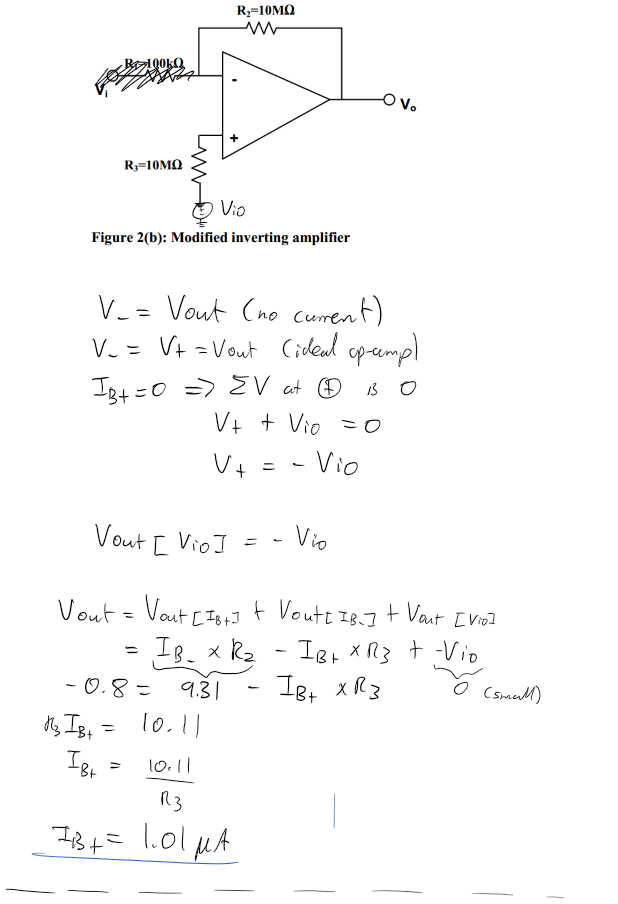
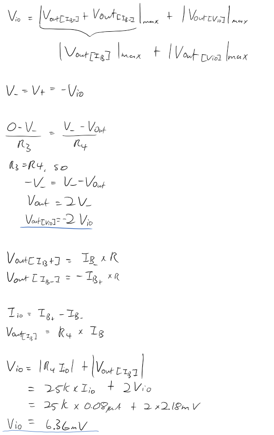
![Untitled picture.png Measurements are conducted on the output voltage of the inverting amplifier under
the following conditions: (i) the input (VD is open circuited and the output voltage is
found to be +9.31 V ; (ii) the input (Vi) is grounded and the Output voltage is found to
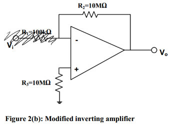
be +9.09V; (iii) the inverting amplifier is further modified by connecting a IOMQ
resistor between the positive input terminal and ground (shown in Figure 2(b)) and the
output voltage is measured to be -0.8V with the input (VD opened. What are the
estimate values of the input offset voltage, input offset current and input bias current
Of the op-amp?
[30 Marks]
Ink Drawings
Ink Drawings
Ink Drawings](Assignment%20One_files/image023.png)
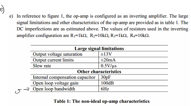
![Machine generated alternative text:
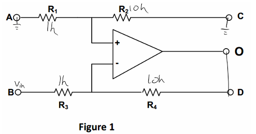
Estimate the bandwidth of the amplifier assuming that the internal
compensation capacitor creates the dominant pole in the frequency
response of the op-amp?
[6 marks]](Assignment%20One_files/image037.png)
![Machine generated alternative text:
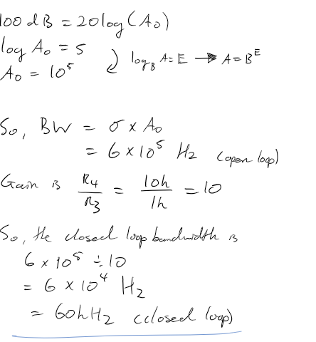
11.
With Vin = and VA=IV , will there be a frequency at which
the output (v o) will be distorted? If so, what is that frequency?
[7 marks]](Assignment%20One_files/image039.png)
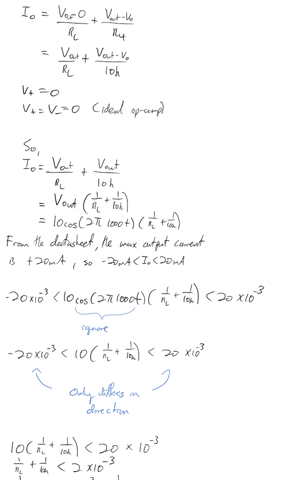
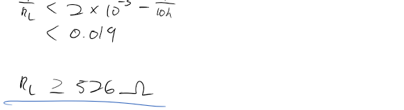
![Machine generated alternative text:
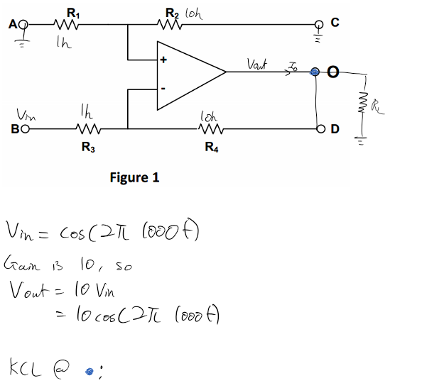
111.
With Vin = VAcos(2a1000t) where VA=IV and assuming that a
resistive load is connected at the output between node Vo and ground,
what is the constrain on the resistive load if the output is to be
undistorted?
[7 marks]](Assignment%20One_files/image042.png)
Assignment One
|
|
|||||||||||||||||
|
|
|||||||||||||||||
|
|
|||||||||||||||||
|
|
|||||||||||||||||
|
|
|||||||||||||||||
|
|
|||||||||||||||||
|
|
|||||||||||||||||
|
|
|||||||||||||||||
|
|
|||||||||||||||||
|
|
|||||||||||||||||
|
|
|||||||||||||||||
|
|
|||||||||||||||||
|
|
|||||||||||||||||
|
|
|||||||||||||||||
|
|
|||||||||||||||||
|
|
|||||||||||||||||
|
|
|
|
|||
|
|
|
||
|
|
|
||
|
|
Created with Microsoft OneNote 2016.