Seminar: Technology Mapping
Contents
Technology mapping is the process in which boolean logic is transformed into circuit components
Why
- Area usage - we want to minimise usage as to not waste resources
- Delay - we want to minimise delay as to run a solution quickly (especially over many iterations)
- Placement and Routability - We want to be able to physically fit the design on a board
Most algorithms prioritise one of the considerations over the other.. how can we create an optimal solution that achieves the best over all considerations
Direct Acyclic Graph (DAG) model
- Node - Logic gate
- Directed Edge - Signal flow
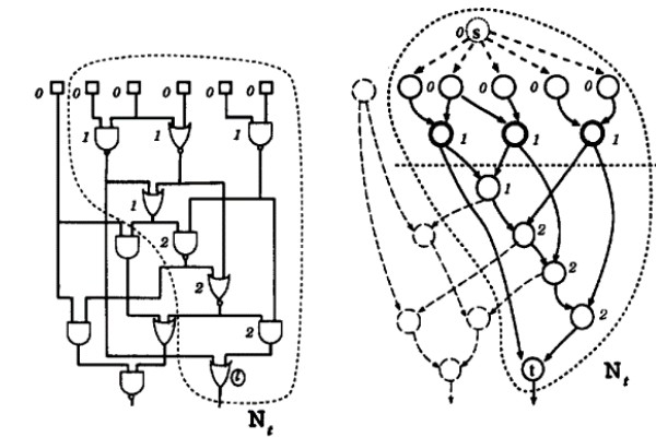
FlowMap
Algorithm to produce a depth-minimsed solution which is delay optimised in polynomial time
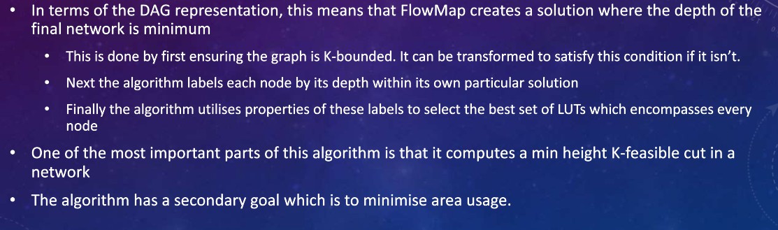
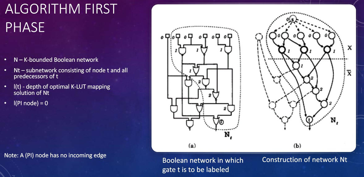
Phase 1: Compute a label for all the nodes
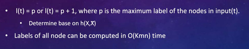
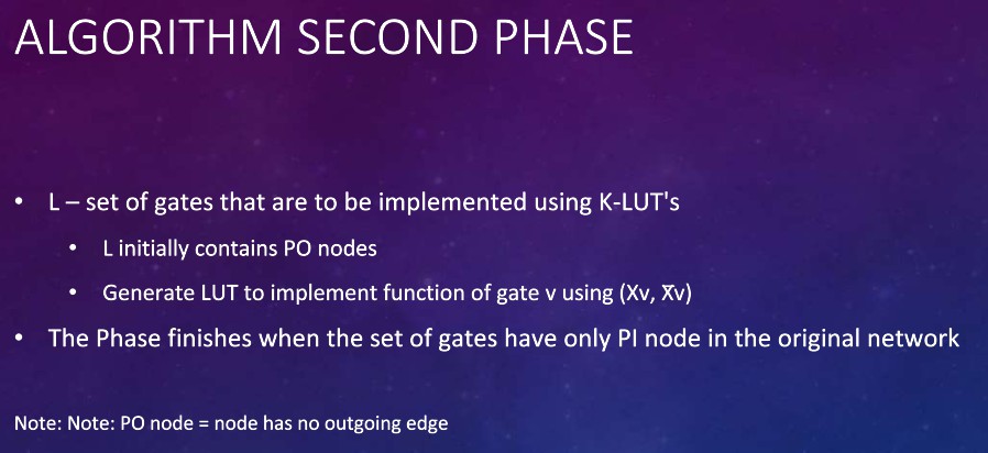
Phase 2: Generate K-LUT
FlowMap Improvements
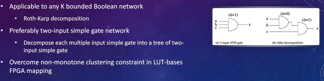
K - number of inputs to the LUT
K-feasible cut - Best way to cut the tree (cutting max K lines)
?