Initial Design Report
Contents

Initial Design Report
Team Orange
Ziyue Lian – z5224346
Andrew Nicholson – z5255137
Arpit Singh Rulania – z5238561
Andrew Wong – z5206677
School of Computer Science and Engineering
COMP3601 – Design Project A
2021 Session Three
1. Introduction
The Learning With Errors (LWE) method is a quantum-robust cryptographic algorithm that aims to address the area of confidentiality of the CIA model during data transmission. With the utilisation of an asymmetric key pair, contents of the encrypted data is only accessible by a single party (the owner of the private key). Through the implementation of an error vector into the procedure, strong cryptographic protection against quantum-enabled computation is achieved. This project aims to implement the LWE algorithm onto an Kintex-7 FPGA board that is able to successfully encrypt and decrypt messages strings.
2. MATLAB Model
An implementation of LWE was developed in MATLAB, to create a model that could be used to explore the rudiments of how LWE functions. This model could then be ported onto the Kintex-7 board, where the ported implementation can be tested against the MATLAB model for correctness and porting accuracy.
A test suite was developed to verify the correctness of the MATLAB model, where the key generation, encryption and decryption were repeated for a large number of iterations. Each test run was designed to execute independently - with the private key, public key, error vector, and sampled public key values all being generated on the fly. Furthermore each test suite was repeated for both M=0 and M=1 cases.
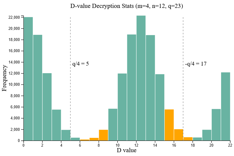
For the parameter set [m=4, n=12, q=23] a sample size of one hundred thousand (100,000) tests provided a successful decryption accuracy of 99.85% (roughly 150 samples failed) for both message bits M=0 and M=1. Figure 2.1 demonstrates that successfully decrypted M values will bias towards D=0 and D=q/2.
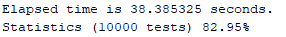
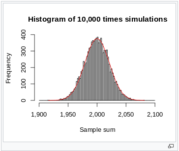
An integration test was also performed given the same parameter set [m=4, n=12, q=23], where a combination of bits (to form the string "Hello, world!" were encrypted and decrypted ten thousand (10,000) times - each test generating their own private/public key pair. Results of the test revealed that 82.95% of the tests successfully decrypted each of the 104 bits, which is of reasonably high accuracy.
(13 characters = 13 bytes = 13 × 8 bits = 104 bits)
A test suite was also written to verify the requirements for an exact private key S to be required for successful decryption of an LWE-encrypted message. Given the same set [m=4, n=12, q=23], when the private key S was not explicitly known (i.e. the private key was altered by one single bit) a tested sample size of one hundred thousand (100,000) tests could not produce a relatively stable output M, where roughly 50% of decrypted D-values were invalid. This verifies the ability for LWE to only be decrypted successfully if the private key is explicitly known.
The LWE cryptographic algorithm has multiple input parameters - specifically the sizes `m` and `n`, as well as the modulo `q`. Additional tests were performed to best understand the impacts of each variable. Values `m`, `n` and `q` were individually modified one at a time to analyse the impact of the variable on the accuracy of decryption.
Modification of m
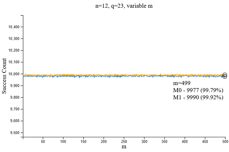
As shown from Figure 2.4 above, given the parameter set [n=12, q=23], the variance of `m` had little to no effect towards the successful rate of decryption. It should be noted that subsequent tests (Figure 2.6.1 and Figure 2.6.2) performed after the completion of this test revealed the same inference.
Modification of n
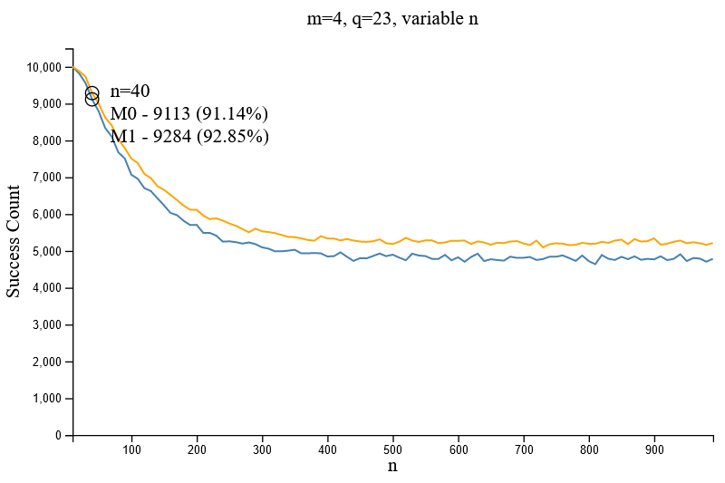
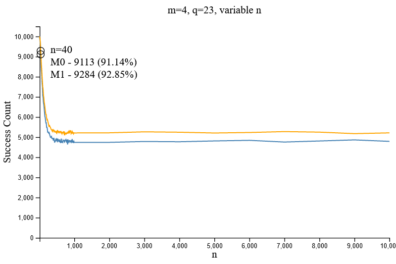
Given the parameter set [m=4, q=23] it was found that the increasing values of `n` dropped the accuracy of a successful decryption (given a known private key). It was also noted that the time required to encrypt and decrypt a message bit was considerably longer with larger values of `n`, however no further quantitative testing was performed to analyse speed impacts. Both observations inferred that the value of `n` should stay small.
Later tests revealed that larger values of `q` were required to maintain the successful decryption accuracy for larger values of `n` (i.e. Figure 2.6.1 and Figure 2.7).
Modification of q
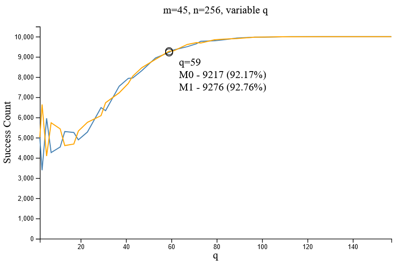
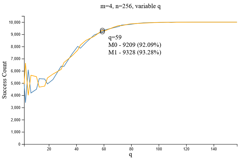
Figure 2.6.1 and Figure 2.6.2 demonstrate the increase in successful decryptions given different values of `q` for the parameter set [m=4/45, n=256]. It can be inferred that large values of `q` are important to ensure the successful decryption of an encrypted message. A comparison between the two above figures indicate the minimal impact of `m` towards decryption accuracy.
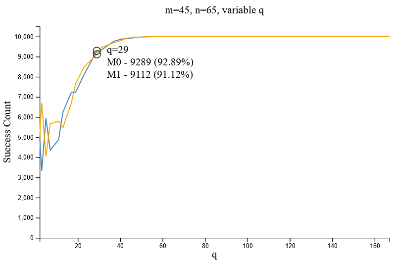
When testing increasing values of q against the parameter set [m=45, n=65], a comparison between n=65 and n=256 (i.e. Comparing Figure 2.6.1 and 2.7) reveals that a higher rate of successful decryptions is achieved when `n` is minimal. Conversely, a larger value of `n` decreases the accuracy of successful decryptions, thus `n` should be restricted to a small value.
Discussion
After the testing and analysis of the decryption accuracy given variations of `m`, `n` and `q`, several findings were established which have helped shape the design decisions for the implementation of the model onto the Kintex-7 FPGA board.
It was noted that modifications to `q` were of the most impact (i.e. Figure 2.7), whereby increasing values of `q` greatly reduces the rate of unsuccessful message decryption given the private key. Hence the HDL implementation should utilise a relatively large value of `q` for optimal accuracy (albeit dependent on the combination of `m` and `n`)
Increases to the size `n` was detrimental (i.e. Figure 2.5.1) as the accuracy of successful decryption (given the correct private key) decreased with increasing values of `n`. Whilst the negative impact on accuracy for larger values of `n` could be mitigated with larger values of `q`, the overall speed of the encryption and decryption routine is adversely impacted from growing values of `n`. As the LWE mechanism functions on a "per-bit" basis (that is, the LWE routine must be performed 8__*__ times per byte) it is of importance that the HDL implementation must use a small value of `n` to operate in acceptable time.
* The ASCII character set (common printable characters) only occupies values 0-127, so each ASCII character can actually be represented as seven (7) bits instead of eight (8). However the time saved by having one less computation pales by an order of magnitude to the speed bottleneck of a large value of `n`
As evident from the above figures, the modification of `m` does not have a significant impact on the accuracy (nor speed) of the LWE method, hence the value `m` can be selected relatively freely.
In conclusion, `q` should be maximised and `n` should be minimised to obtain optimal accuracy and speed for the LWE routine.
Future Work
The current MATLAB model incorporates an exact multiplier, whose computation time is slower when compared to an approximate multiplier. When the future MATLAB model that features an approximate multiplier in lieu of the exact multiplier is created, it will be worthwhile to perform timing tests to quantitatively compare the performance increase.
3. Hardware Design Rationale
3.1. Design Goal
The proposed feature implementation of LWE should achieve the following requirements
- Support modulo values `q` up to 65535
- Support 16-bit wide operations
- Generate a private key
- Generate a public key
- Encrypt a message bit
- Decrypt an encrypted message
- Encrypt a stream of serialised bits from a file
- Consume a minimal board area and resource footprint (e.g. I/O, CLBs)
3.2. Design Choices and Assumptions
Board Selection
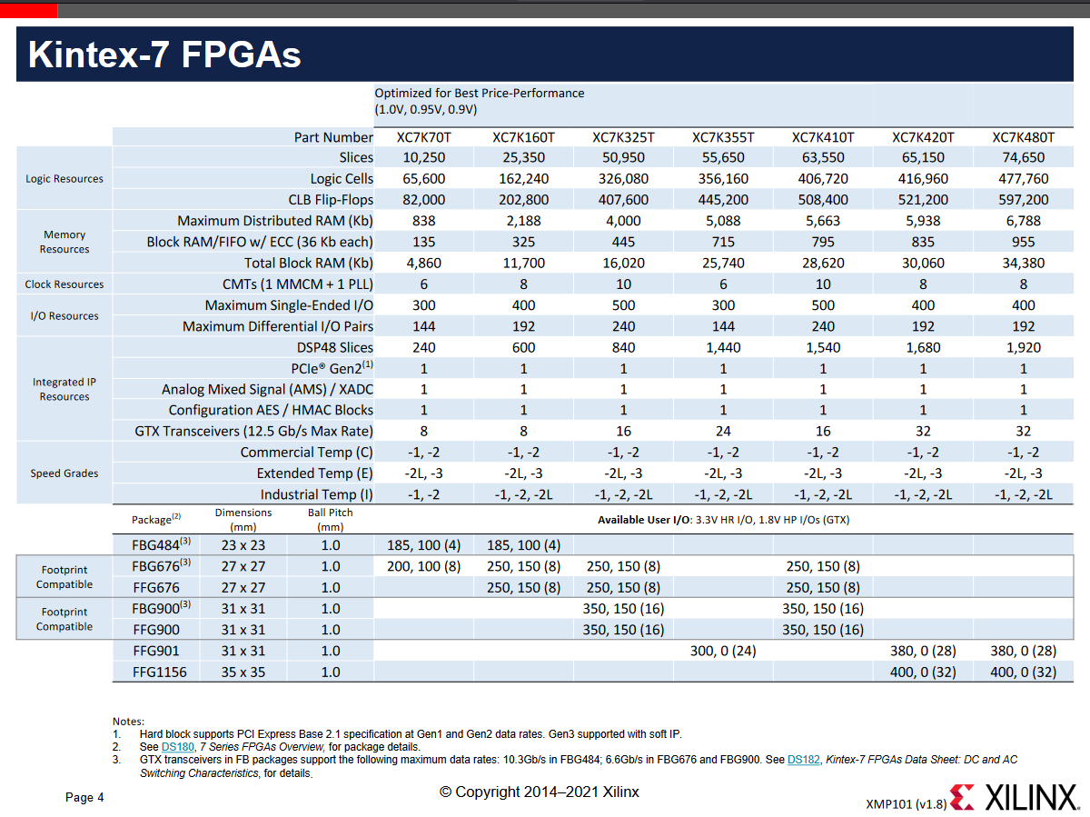
Within the Kintex-7 series of FPGA chips, the xc7k70tfbv676-3 was selected to be used for the implementation of the design. This is an entry-grade chip within the Kintex-7 series, with a logic cell count of 70,000 and available pin count of 676, which is of minimal size as when compared to more performant chips in the series. Consideration towards prioritising the reduction of area size and resource utilisation was sought after, whereby the minimal resource footprint of the implementation would guarantee that the designed system can be easily integrated into other packages without concern for I/O availability.
HDL Language Choice
As the majority of Team Orange's members were more comfortable with VHDL than Verilog, VHDL was the selected hardware description language to be used. Whilst Xilinx provides interoperability and cross-language compatibility to allow usage of both VHDL and Verilog; a singular language (VHDL) was enforced to establish a maintainable and shared understanding of the codebase.
Design Rules and Assumptions
Multi-cycle components will accept an input clock signal `clk`, and synchronise their operation to the rising edge of the clock. All clock signals will be backed from the same clock provider, as to provide unified synchronisation.
Functional components (that is, components which perform an atomic function) that manage an internal state (i.e. for the execution of a multi-cycle task) should set up their state during the assertion of the reset signal `rst`, which, when deasserted will allow the component to execute on the very next cycle.
To assert the completion of a functional component, a `ready` bit is to be implemented as an output signal. Once asserted, the functional component's output signals and internal state should no longer vary, and remain constant until the reset signal is asserted
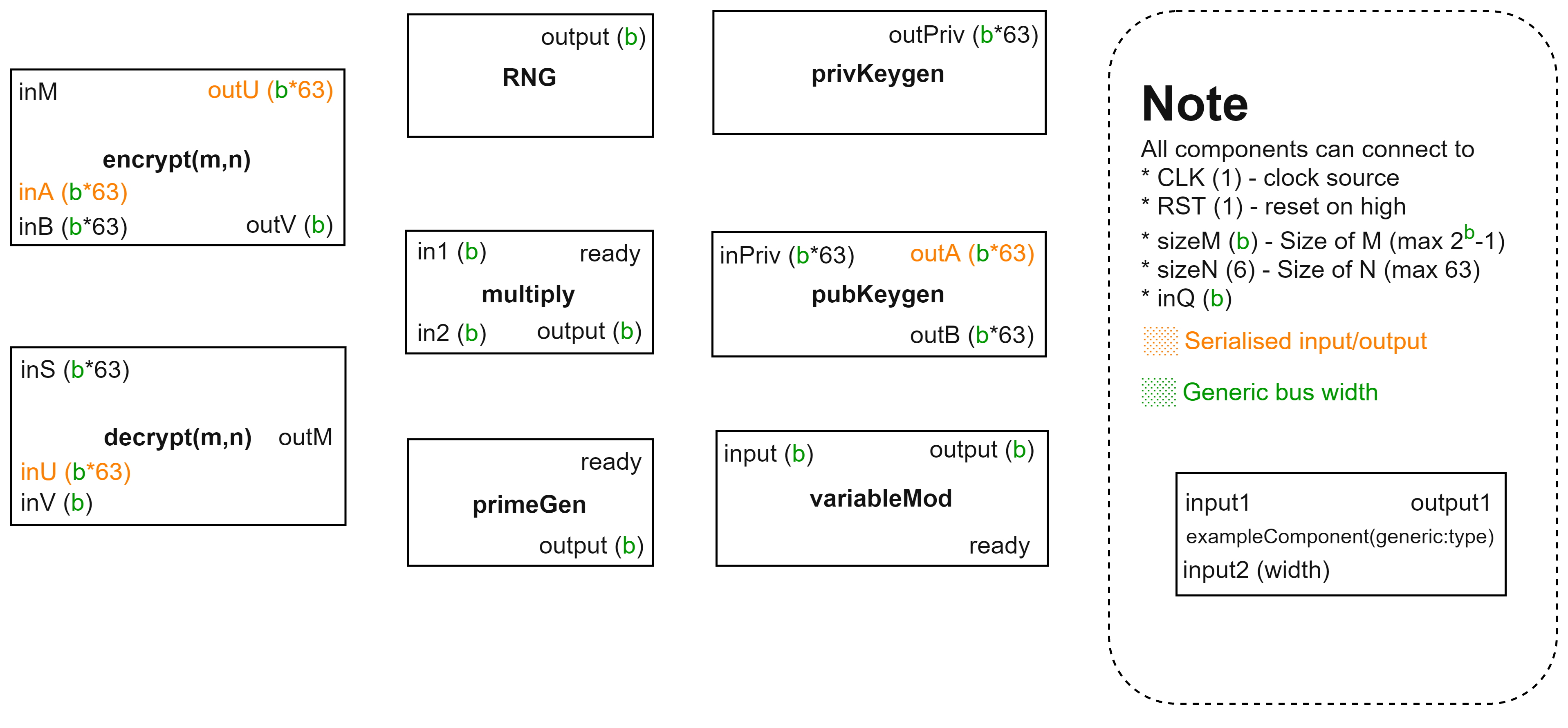
Components that require size `m`, or size `n` of a vector matrix should accept an input signal `sizeM` / `sizeN`. Similarly, components that are functionally dependent on the modulo value `q` should accept an input signal `inQ`
As supported by prior MATLAB modelling analysis (Figure 2.5.1), size `n` should be a small number - but at least 32 (as required per assignment specification). To allow flexibility (should the user want to encode a value larger than 32, the implemented LWE design will accept 6 bits for the signal `sizeN` (max value of 26-1 = 63).
For integrations of the LWE implementation in specific `b`-bit systems, the board area requirement will be optimised by providing the integrator a bus-width parameter `width` (whose default is 16). For example, when integrated with a bus-width of 8 bits, the LWE implementation synthesis will remove redundant I/O lanes that would otherwise only be used on a 16-bit system.
4. Datapath Design
5. Random Number Generation
5.1 Random Number Generator using LFSR
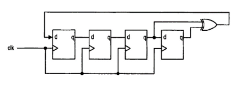
We used the Linear-Feedback Shift Register (LFSR) as our Random Number Generator. An LFSR is a cascade of flip-flop circuits, which takes in a linear function, such as exclusive OR, as the input.
5.2 Seed Generation for RNG
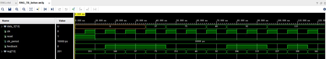
The random number generator takes in a fixed seed as an initial input that is passed into the LFSR (linear feedback shift register). The output is then parsed through the LFSR again multiple times to get the random numbers every clock cycle. This pseudo-random sequence of numbers is however the same each time the rng module is called.
To resolve this issue, the most simple and effective solution was to change the initial seed that is used each time when the reset signal is asserted to ‘1’. To get a different seed each time, the current date and time is extracted as a standard logic vector, and the bits are manipulated to create a random initial sixteen bit seed for the LFSR.
5.3 Random Prime Number Generation
For the random prime number generation, we created a separate array to store the prime numbers, and make use of the result of the random number generator (a single random number but within a smaller range) as the index of the array, to select a specific prime number to output. By precalculating the prime numbers (which by nature do not change in 'prime-ness'), the required board area can be minimised as no components will be required to perform a primality check
5.4 Consideration of Alternate Methods
Other methods that were considered for random number generation included the MT19937 Mersenne Twister, the Xoroshiro128+ PRNG algorithm, and the Trivium PRNG algorithm. However after carefully considering and analysing each of these algorithms, we found that LFSR uses the least number of FPGA resources when compared to the other methods. Furthermore, further investigation into the Xoroshiro128+ algorithm revealed that its randomness was only optimal for extremely large number ranges, in the magnitude of 128 bit and larger values. This led us to choose LFSR as the PRNG algorithm paired with the current date and time combination as a random seed.
6. Multiplier
6.1 Exact Multiplication
As an initial design, the novel repeated addition algorithm was implemented in VHDL.
Given a large multiplicand `x` and multiplier `y`, the repeated addition algorithm would require `x` clock cycles to complete. This is evidently unideal, especially for larger n-bit multiplications (i.e. 65535 × 50 would take sixty five thousand clock cycles).
A possible optimisation could be implemented by switching the multiplicand and multiplier around when required, as to repeat the loop only as many times as the smallest of the terms - for example 50 × 65535 would only take 50 clock cycles. However this optimisation fails to improve the time cost for multiplications of two large numbers; as 65535 × 65534 will still take sixty five thousand clock cycles despite the choice of multiplicand and multiplier.
Consequently, research was performed to investigate alternative methods of multiplying two numbers together that were more efficient (speed-wise) than the repeated addition algorithm. The traditional 'long multiplication' was examined however not attempted in implementation due to its known time complexity of O(n^2).
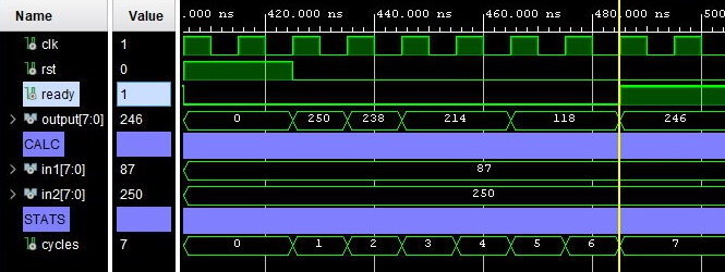
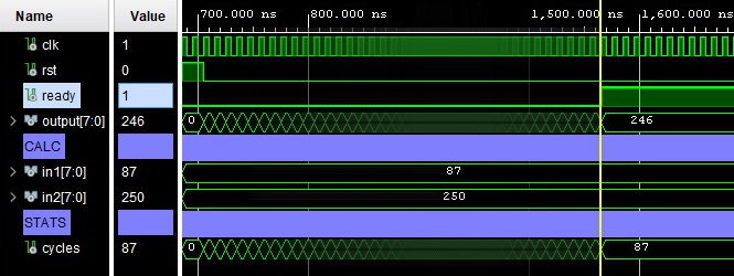
In researching more time efficient multiplication algorithms, an algorithm was found that would operate in a time only bound by the bit-size of the multiplication terms. This algorithm revolved around multiplying an intermediate result by two every time the intermediate multiplicand was divisible by two when halved, else simply performing a binary addition. As seen in Figure 6.2, the algorithm was able to compute 87 × 250 in 7 clock cycles, which is 1240% faster than the novel approach. The pseudo code for such an algorithm is as found below
Due to the nature of how the aforementioned algorithm internally operated on its n-bit terms, a guarantee of at most `n` clock cycles of execution was discovered, whose bounds held true for any n-bit number regardless of the value of the multiplicand or multiplier. This would ensure that the multiplication of the 16-bit values 65535 × 65534 would only require a maximum 16 clock cycles of execution. Additionally, as compared to the prior novel approach - no reordering of the multiplicand and multiplier values were required.
Further research on faster multiplication methods revealed that a plethora of other "fast multiplier" algorithms exist, inclusive of Karatsuba's, Schonhange & Strassen's, Booth's, Toom-Cook's, and the most performant (currently) algorithm by Harvey and van der Hoeven - which incurs a time complexity of O(n log(n)). Whilst these algorithms exhibit efficiency in multiplying large numbers, they do not add much benefit for the multiplication of small numbers. In fact, the implementation of these algorithms would have a larger resource footprint (due to their internal multipliers and storage blocks) which would dramatically increase the board area. As minimising the board area is a goal for this LWE implementation, it was decided that these sophisticated multiplication algorithms would not be implemented.
6.2 Consideration of Hardware Optimisations
Regardless of the multiplication algorithm implemented, there exists a hardware bottleneck where a clock cycle must be used to wait for the setup and deassertion of the `rst` signal, and another cycle for the polling of the `ready` signal. As a result, two extra clock cycles are required for each additional multiplication that is required by the LWE design.
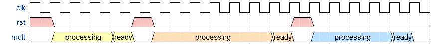
For example in Figure 6.2.1, when three independent multiplications are processed one after the other, the LWE module would have to deassert the `rst` signal three times before the processing begins on the next clock cycle. Before asserting the next `rst` signal, the system must wait for `ready` to be asserted.
As the additional control signal clock cycle delays were of a hardware nature, focus was shifted away from software optimisations and onto hardware optimisations. In an attempt to reduce the number of clock cycles, parallel and pipelined processing paradigms were investigated.
Parallel Processing
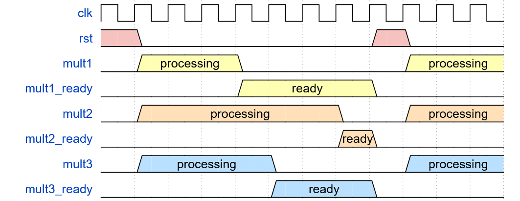
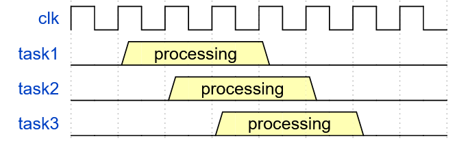
Parallel processing of multiplication operations involve having multiple instances of the multiplication component within the LWE module. This allows for each multiplier to independently operate on their parameters simultaneously, allowing for a higher throughput of data. Compared to serial multiplication (as seen in Figure 6.2.1), the time it takes to complete the same task in a 3-parallel multiplier is considerably less, requiring only 8 clock cycles as compared to 19 clock cycles for a 3-serial multiplication.
There are two disadvantages of parallel processing of multipliers, with the first disadvantage being the increased resource usage of the available board area, as each multiplier will require their own I/O and internal components on the FPGA. This will adversely impact the goal to minimise the board area for the LWE design.
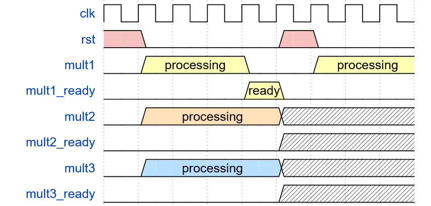
Another potential disadvantage of implementing a parallel design is the delay for a completed worker of a parallel set to begin a new task. In Figure 6.2.2, whilst mult1 has been marked as `ready` the multiplier must wait for both mult2 and mult3 to complete before the parallel set can be reset and be given new parameters. This is as a result of synchronisation locking, where all tasks in a parallel set must be completed to ensure that a new task will not corrupt the state of another task. If a multiplier is started prematurely before the completion of all the parallel workers in the active iteration, the internal states of the other multipliers can be corrupted, as seen in Figure 6.2.3.
Whilst it is possible to give each multiplier their own queue, this paradigm issue will inevitably need to be managed elsewhere within the design, whether it be a buffer or a synchronisation lock. The risk of corruption due to unlocked task synchronisation is dependent on the nature of the parallel data; if the parallel set is operating on data that must be treated as a whole, then synchronisation must be addressed. Conversely, for unbound data this issue is not of concern.
Pipelined Processing
Pipelined processing refers to the simultaneous execution of several instructions where each instruction is at a different stage of the Fetch-Decode-Execute cycle. Pipelined processing allows for hardware that is unused by a former instruction to be utilised for subsequent instructions, even whilst the former instruction has not yet completed. The pipelining of instructions compared to the serial chaining of instructions dramatically reduces the required clock cycles to complete tasks.
In application to optimising the multiplication hardware, it was concluded that pipelined multiplication would be difficult to implement, as the multiplication process is already atomic. Furthermore, pipelining refers more-so to processor design than in application to optimising an individual component.
Discussion
Given the project requirements to be able to process and multiply matrices (i.e. Public key A of size m × n), it was deemed necessary to incorporate some parallel processing into the multiplier despite an increase in board area - as the speed improvements (in this instance) were considered more important.
6.3 Approximate Multipliers
The implementation of an approximate multiplier is crucial in decreasing the required clock cycles for a multiplication, especially when the results of the multiplication do not need to be exact (such as the least significant bits of a large n-bit multiplication having little effect on the magnitude of the product). Replacing the current exact multiplier implementation with an approximate multiplier will be the focus of the latter half of this project's schedule.
The approximate multiplier will likely share the same port interface as the exact multiplier, having two input signals, an output signal, and a ready signal.
7. Modulo
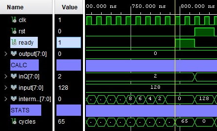
Similar to the multiplier component, a basic modulo algorithm was initially implemented, where a divisor was constantly subtracted from a dividend until the result was less than the divisor. In the example above (Figure 7.1), the operation 128 % 2 consumed 65 clock cycles; for larger n-bit values it was evident that this novel algorithm was suboptimal.
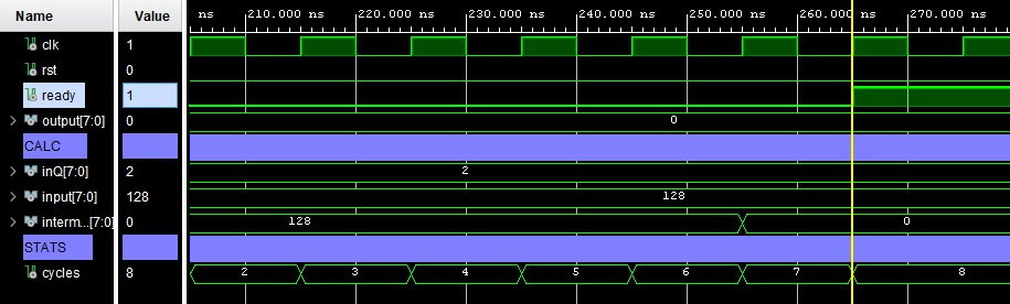
Likewise with the bit-shift multiplication algorithm, a bit-shifting modulo algorithm was implemented, where larger multiples of the divisor (in powers of 2) were subtracted from the dividend before smaller multiples. For example, subtracting `4x` consumes one clock cycle; compared to four clock cycles being required to subtract `x` four times.
Consequently, this algorithm achieved a speedup of 812% for a 128 % 2 operation.
Whilst this algorithm doesn't guarantee a maximum execution duration of `n` clock cycles for an n-bit operation, there are still substantial performance improvements.
Special case optimisations, such as cases for when the divisor is 1 or 2 could be implemented, however these cases are extremely unlikely to be encountered within the LWE design, which will only utilise the modulo operation against fairly large prime values.
8. Secret Key Generation
The secret key generation module outputs an array of 16 bit integers that acts as the hidden private key for the public key generation. This secret key takes a specified number of randomly generated values and stores them as an array for use in public key generation and decryption.
For modularity the number of rows in the output secret key vector is declared as a generic. This number, n, is related to the number of columns required in the desired A matrix. The implemented LWE design can function with n values up to 5 bits (i.e. 32), as to meet the minimum requirements of 4, 8 and 16 values, whilst still allowing further modularity up to 32 rows. It should be noted (see Figure 2.5.1) that the value n should be minimised for optimal performance in speed.
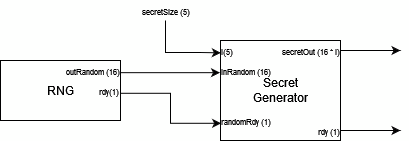
On each positive edge of the RNG module’s clock signal `clk` the secret generator will sample the RNG output and populate the output array. Once the entire secret has been generated then the ready signal will be set high to alert other modules that the secret is available.
9. Public Key Generation
9.1 Generating A Matrix
Generating the A matrix is similar to the generation of the secret key. The RNG module is sampled on positive-edges of the ready signal and is used to populate the entire matrix.
Under the considerations of the project specification the matrix A occupies 16*_mn_ bits. To reduce the space required for outputting the result of the generator the output will be serialised. The output is thus a 16_m_ std logic vector which will require _n_ output cycles to transmit the entire A matrix.
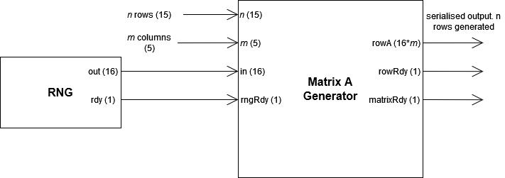
At the completion of every row the output of rngRdy is set high to alert other modules that an entire row of A is available on the output rowA bus. Once n rows have been completed the matrixRdy output is set high and the process is halted.
The main controller unit will store the complete output of the A matrix as a part of the public key to be sampled by the encryption scheme.
9.2 Generating Error Vector
The generation of an error vector requires a modified RNG module as the standard module only produces a uniform distribution. The error vector values must be sampled from a normally distributed random function.
In the future this error vector is made redundant by the introduction of the approximate multiplier, as the error is intrinsic to the calculation.
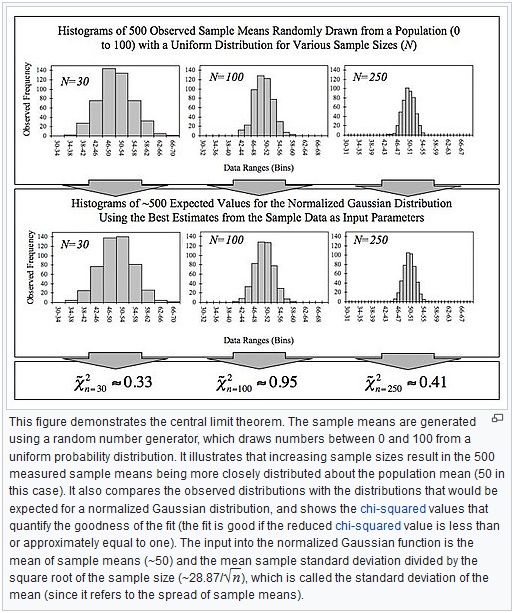
One method for the generation of normally distributed random numbers is through the use of the central limit theorem. The central limit theorem concludes that an approximate normal distribution can be achieved by summing independent random numbers. As such we can take the existing RNG module as an input to the normally distributed error generator.
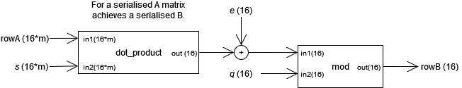
9.3 Generating B Matrix
To generate the B matrix a multiplication between the matrix A and the secret key vector must be calculated, to the result of which an error must be added. Each element of the resulting vector must then be passed to the modulo operation with the decided prime value q as the divisor.
The serialisation of the matrix A reduces the circuitry required to compute the matrix multiplication. Each row of the A matrix is treated as a vector and the dot product is performed with the secret key s. Results of the dot product performed on each row of A have an error added and then modulo performed. This results in the serialised output of the column vector B.
Further efficiencies can potentially be obtained through the implementation of an approximate multiplier as this will inherently add an error factor when calculating the product of the A matrix with the secret key s.
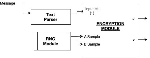
10. Encryption
The encryption module works in 3 main steps. The first step is to parse the input that is to be encrypted. The input is a message that is represented as a vector of std_logic bits which is just the ASCII representation of the message in binary. Each bit from this input is then passed through the encryption algorithm. The encryption algorithm is carried out in two steps which involve calculating u and v respectively.
To calculate u, the matrix A has to be sampled randomly. To do this, the random number generator module is called as a component and the same indices produced are used to sample the matrix ‘B’. Next the sum of the ‘A’ samples’ is calculated and the result is a one row matrix, every element of which is then passed into the modulo function to produce the u matrix.
To calculate v, the sum of the ‘B’ matrix sample is calculated. The matrix was sampled in the previous step using the RNG module when matrix ‘A’ was sampled. This sum is then added to the prime number q divided by two only when the message bit is ‘1’. If the message bit is zero then nothing is added to the sum. The output is v.
The encryption module then passes the matrix u and the number v to the receiver who can use the decryption module to decipher the message.
The input to the encryption module is serialised, so it received the public key (‘A’,’B’) of 16*m bits, ‘n’ times. Random incoming rows are saved and some rows are dropped which is decided by the random number generator. Once the encryption of the message has been completed, the output pair (u,v) is also serialised and is sent to the decryption module ‘n’ times. Serialisation is done to improve the storage efficiency of the algorithm on the hardware.
11. Decryption
Decryption of encrypted messages is given by the expression D = (v - S·u) % q, where
- D is a decrypted value
- S is the secret key (size `n`)
- u is one part of the encrypted data
- v is another part of the encrypted data
- S·u is the dot product of S and u
Once a message is decrypted, it can be decoded given the constraints that message M = 0 when -q/4 <= D < q/4. Considering the unsigned nature of values in the LWE design, this inequality can be simplified and inverted to produce the conditional inequality M = 1 when q/4 <= D < 3q/4.
To further simplify this inequality, q/4 could be subtracted from the inequality to produce the conditional inequality M = 1 when 0 <= D - q/4 < q/2, or simply M = 1 when D - q/4 < q/2.
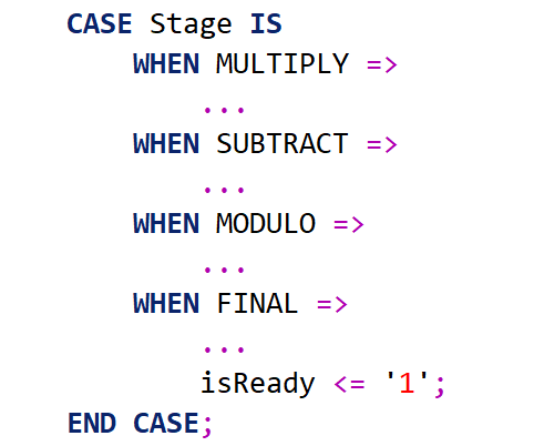
A finite state machine-like structure was implemented to control the behaviour of the decryption component during its several stages (i.e. multiplication, subtraction, modulo and comparison). This decoupled the requirement for flag/state variables, which consequently simplified the development and maintenance of the component.
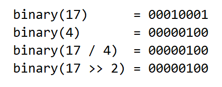
To efficiently calculate q/2, bitwise arithmetic can be used in lieu of a division component by logically shifting the bits of q to the right by one place (q >> 1). Similarly, a logical right shift of 2 bits for the bits of q will produce an equivalent result to q/4.
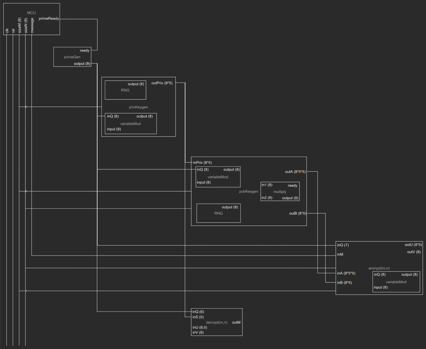
12. Main Control Unit (MCU)
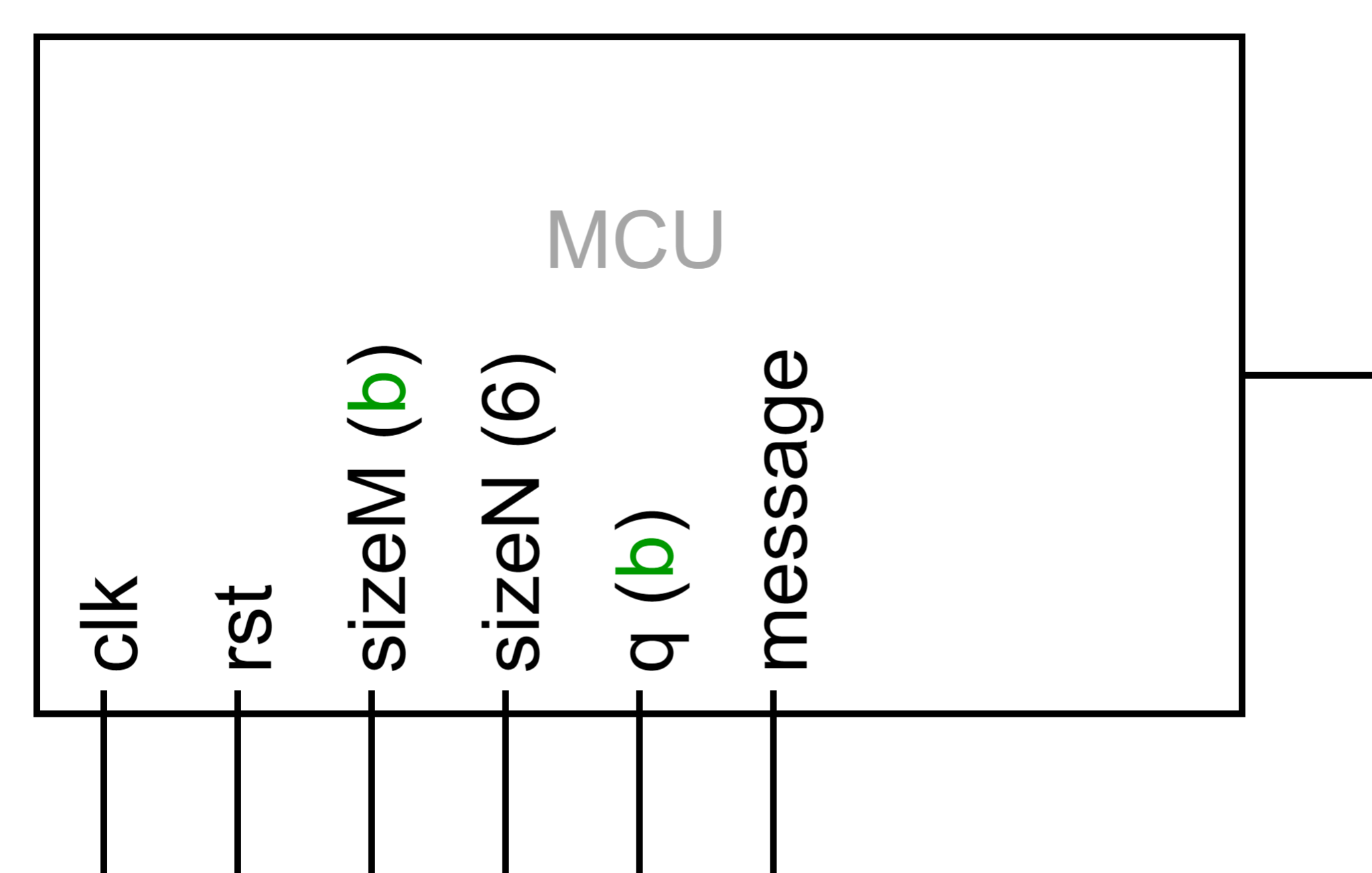
The main controller unit (MCU) is responsible for interfacing with each main component of the LWE design, such as the (de)assertion of the `rst` signal, as well as the seeding and retrieval of data to and from other components.
The MCU is also responsible for providing the clock signal (`clk`), variables `sizeM` and `sizeN`, the message bit to encode, and modulo value `q` as global signals that can be connected to the required components. A stream of bits (i.e. bytes of a string) will be able to be encrypted and transmitted through the MCU, whose source can originate from a text file.
13. Testing Components
Unit testing of individual components was performed through the creation of testbenches in Vivado. These tests were designed to verify the correct functionality of the implemented VHDL code, and to provide insight into critical paths and delays for future optimisations. For the majority of functional components, the tests sought to validate the accuracy of the function as well as the stability of the component, such as the internal state becoming immutable when the ready signal is asserted.
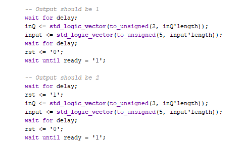
For each testbench, a standardised approach routine was devised to consistently test components between files. Particularly, each individual test should contain an initialiser, trigger and wait stage, each separated by some form of time delay.
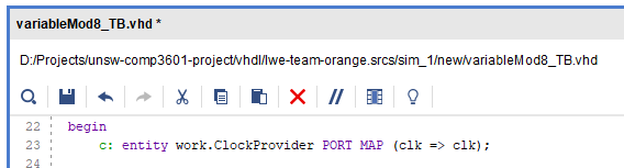
To achieve consistent results between tests, and between components per test, a standardised clock period of 10ns was selected, as to ensure that sufficient time was allocated per cycle for each component's cycle to wholly complete. During a synthesis of the system (in its partially completed state), it was discovered that a period of 2.961ns (~338 MHz) was the fastest permissible clock cycle period for operation without encountering any jitter or abnormalities.
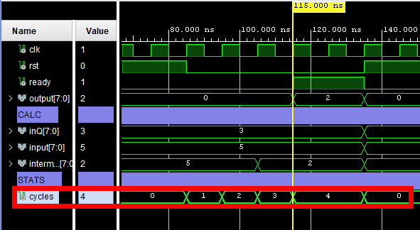
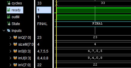
Whilst speed efficiency is not the principle of focus, it is still of relevance and of best interest to perform layout-independent design optimisations to decrease the number of cycles required for components to complete. To assist in the benchmarking and optimisation of cycle count, a cycle counter was incorporated into each testbench to log the number of cycles that have elapsed during the duration between the deassertion of the reset signal `rst`, and the assertion of the ready signal `ready`. Upon graphical inspection of the resultant waveform, this auxiliary measurement provided fast and straight-forward information about the component's runtime duration without requiring the manual counting of clock cycles.
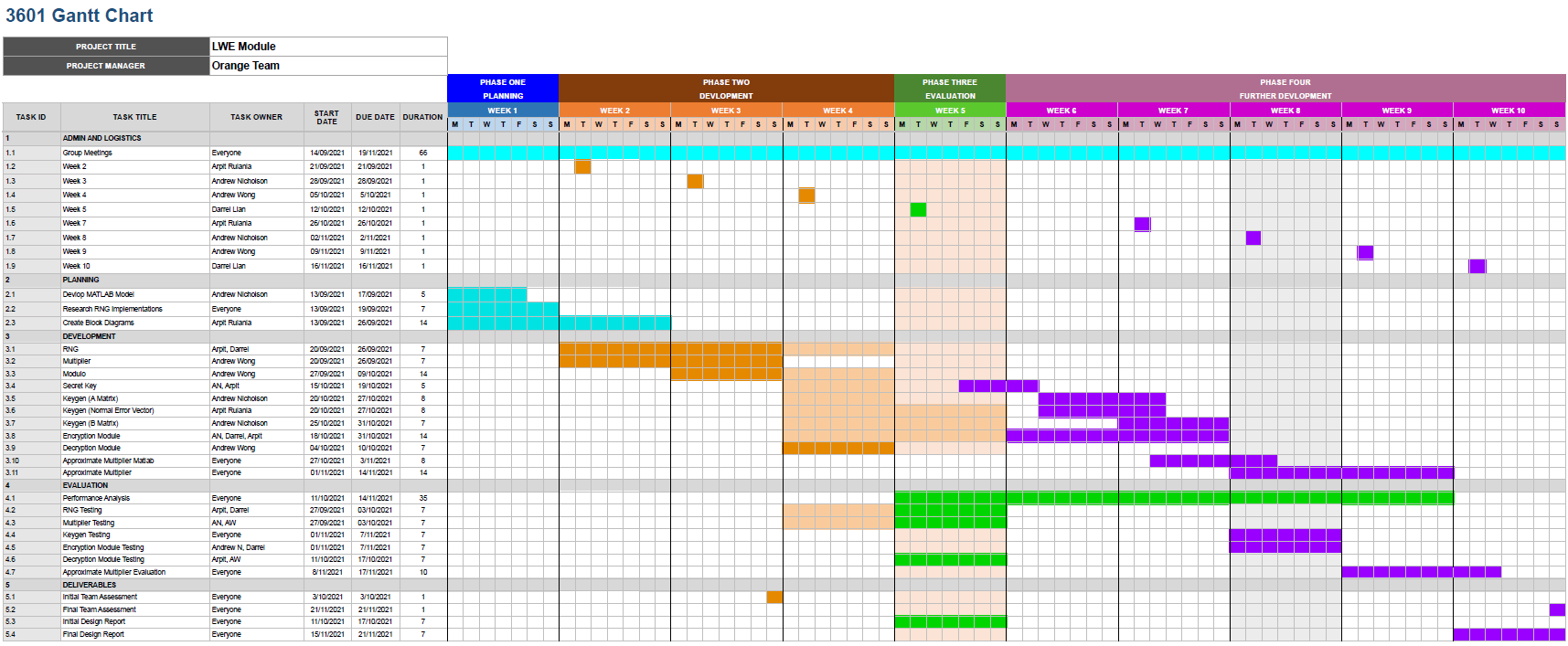
14. Planning and Timeline
This project is divided into four major phases. The first phase of the project was set to take place in week one where the initial plans for the project timeline were first laid out. Following that in the next three weeks was the development phase. This phase was mainly aimed towards getting a rough implementation of the different modules completed. Once that is complete phase three moves the project towards evaluating the current efficiency of the implementations of the module and improving the performance. Finally the last phase was created for further development giving the team sufficient time to develop the project further and improve on the current progress made up till that phase.
Going forward into the last five weeks of this project, the plans to complete the additional modules that are crucial to the LWE implementation are laid out in the gantt chart. Phase four of the development lifecycle of this project consists of completing Key generation modules and the encryption modules. Once that is complete, further development into using approximate multipliers will be carried out and the evaluation of the different implementations of the approximate multipliers is reserved for week nine and the start of week ten. The final week is reserved for tying up the loose ends and finalising the implementation as a whole.
Group meetings are scheduled to occur every Monday and Friday of each week, where a standup is conducted and each group member talks about their progress on their respective part of the project and is assigned new tasks as required. These group meetings are extremely crucial to the smooth functioning of the team and the completion of the project.
The LWE project has been divided into eleven major modules. These modules are shown in the development part of the Gantt chart below. This work was equally divided amongst the group members at the start of the project in week one.
15. Conclusion
LWE is aimed toward creating a more secure method of encrypting data for public key cryptography that is quantum secure. So far we have shown that the LWE is effective using MATLAB and aim to improve this algorithm with engineering design considerations in mind. Completing the design and optimising it are the tasks that will be completed in the next phase of this project. To conclude this project has been planned out meticulously and all of the progress made till now has been in accordance with our Gantt chart.
16. Appendix
2.1 - MATLAB Model
| |
2.2 MATLAB Integration Test
| |