Course Summary
Contents
Boolean Algebra
Truth Table
A truth table describes the boolean algebraic value of (an) output(s) given differing input values
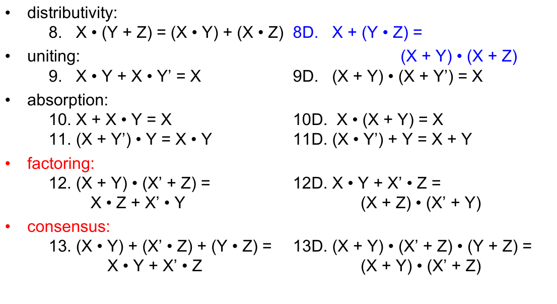
Duals
The dual of an algebraic boolean expression is a sort of complement form that infers the same meaning.
- OR <-> AND (Switch AND and OR statements)
- 0 <-> 1 (Switch 0 and 1 values)
Karnaugh Map
A Karnaugh Map helps to simplify functions by reducing the number of required terms to achieve the same function.
- Set the columns as the most significant variables
- Set the rows as the least significant variables
Note: The ratio of columns to rows is unimportant (but it's good to attempt to keep them relatively 1:1)
- Karnaugh Maps are grey-encoded - When laying out columns and rows, the next column/row can only differ by one bit.
- Do: 00, 01, 11, 10
- Don't: 00, 01, 10, 11
To use a Karnaugh Map, find simplified conditions for which a set of values are all 1 (or 0 for maxterms).
- Note: A Karnaugh Map forms a torus - the end of a column/row is connected to its start
- Note: It may be possible to combine the Karnaugh Map with other similar circuits, which can reduce the number of required components
Rules
Circuits
Costs
The "cost" of a circuit can be explored as the sum of the number of gates and the number of gate inputs.
cost = #gates + #gate_inputs
This is a good measure of cost as less gates will require fewer transistors.
When dealing with inverted input values, those gates are not counted
Circuit Synthesis
Given a truth table, an expression can be formed from the sum of f=1 entries.
minterm- a product term (AND) where each term appears only once (regardless of complement)maxterm- a sum term (OR) where each term appears only once; a complement of the minterm
- Sum of Products - Sum of
minterms- Canonical SOP - If each product term is a minterm
- Product of Sums - Product of
maxterms- Canonical POS - If each sum term is a maxterm
Physical Circuit Design
There is a physical limit to the number of inputs that they can have - for example: propagation time. As such, there are a number of ways to 'refactor' the design.
i.e. Decrease the number of inputs for each gate, but add a second gate
Circuit Devices
The speed of a circuit is bound by the longest delay along the paths in that circuit.
The longest path is called the critical path, and its delay is known as the critical path delay
Multiplexer / Mux
Switches an output given a set of inputs.
$f = \overline{s}\cdot{x_0} + {s}\cdot{x_1}
Shannon's Expansion Theorem
Mux implementations of logic functions require that a given function to be decomposed with respect to the variables that are used as the select inputs
Variable split -> $f(w_1, w_2, ...) -> w_1f_{w_1}(1, w_2, ...) + \overline{w_1}f_\overline{w_1}(0, w_2, ...)$
We can also split multiple variables - breaking them into permutations of terms
Gates
NAND and NOR gates are used in favour of AND and OR gates due to the nature of how they are built. NAND and NOR gates pull the input voltage to zero if certain cases (given by their functionality) are met. As a result of this implementation, AND and OR gates get their operation through gating the NAND/NOR gate with a NOT gate - which requires an additional 2 transistors.
NOT Gate
- $\overbar{x}$
- Requires 2 transistors
NOR Gate
- Requires 4 transistors
NAND Gate
- Requires 4 transistors
AND Gate
- Requires 6 transistors (AND + NOT)
Gate Conversion
NAND Conversion (In a SOP network)
- Add bubbles (
NOT) to the output of everyANDgate - Add bubbles (
NOT) to the input of everyORgate - Replace
ORgates with bubbled inputs toNANDgates
NOR Conversion (In a POS network)
- Add bubbles (
NOT) to the output of everyORgate - Add bubbles (
NOT) to the input of everyANDgate - Equalise bubbles (Cancel out double-
NOT) - Replace
ANDgates with bubbled inputs toNORgates
Adder Circuits
Adds bits together giving an output, and a carry bit.
Several adder components can be stacked together to create an n-bit adder.
Carry Lookahead
- A carry needs to be generated if
g = ab = 1 - Otherwise, a carry needs to be propagated if
p = (a + b)cin
An additional carry-lookhead logic block takes in these values of g and p for each bit-block; allowing future adders to take the g and p values of other blocks.
$c_i = g_n OR p_n$
- Carry bits produced after 3 gate delays
- Sum bits produced after 4 gate delays
- Each stage requires another AND gate with another state
Calculation: Minimum 4
Subtraction Circuits
Add the two's complement of a number X to perform a "subtraction of X" operation
Multiplication Circuit
Add n time
Division
Move scope of dividend until divisor is subtractable
Encoders and Decoders
Turning data from one form to another
An $n$-bit signal could be turned into $2^n$ outputs, allowing a 'one-hot encoded' value to be formed (only one output is active at any given time)
Latches
Respond while clock is high
- RS-Latch - Latch responds when clock is high
- Undefined behaviour when
SandRare both asserted
- Undefined behaviour when
- D-Latch - Latch responds when clock is high
Flip-Flop Circuits
Respond only during transitions of the clock edge
- D-Flip-Flop - Set to D on clock transition
- T-Flip-Flop - Toggle result when T is high
- JK-Flip-Flop - (Most versatile one) - Toggle, set, or hold
Registers
A register is a collection of flip-flop circuits that are grouped together
Shift Registers
Shift registers shift the incoming data either left or right
Parallel Access
Allows a shift register to be loaded in serially (by shifting), or all at once.
This is done by muxing the D-flip-flop input.
Three State / Tri-State Buffers
Output is of a high impedance if $c = 0$, else output is the value of the input $i$.
Counters
Store values, increment and/or decrement.
Increasing logic is performed by an AND gate (only increment if both previous register and register before that (...) are asserted)
Implementation: Use the same clock signals!
Clocks
Clocks are used to synchronise operations
Circuit Delays
Devices take time for their outputs to be asserted correctly (floating values, physical connections, gate delays).
- Propagation Delay - $t_{cQ}$ - Time taken for the output to reflect an input change
- Beginning of input transition (ie clock) to output change
- Setup Time - $t_{su}$ - Time needed for the input to be stable prior to the triggering clock edge
- Hold Time - $t_{h}$ - Time needed for the input to be stable after to the triggering clock edge
$$ T_{min} = \frac{1}{F_{max}} $$
$$ T_{min}$ = max(t_{cQ}) + t_{NOT} + t_{su} $$ $$ F_{max} = \frac{1}{T_{min}} $$
Therefore, max clock speed is $ F_{max} $ Any faster, $t_{su}$ will not be satisfied
To determine the shortest delay from any positive clock edge to flip-flop input.
$$ min(t_{cQ}) + t_{NOT} > t_h $$
Clock Skew
Due to wire delays, the same clock edge may arrive at different times.
FPGA boards have special clock distribution networks that minimise the time difference of received clock edges.
- Positive Clock Skew can be beneficial - signals arrive earlier than expected; can calculate earlier
- Negative Clock Sew is often harmful - signals arrive later, increase delay, reduce max frequency
Synchronous Circuits
- Sequential Circuit - output depends on past inputs and states, and present inputs
Sequential circuits that use a clock signal are known as synchronous sequential circuits (FSM)
- Moore circuit - Output state depends solely on the current state ("step by step")
- Mealy circuit - Output state depends on the current state and the current inputs
- State Diagram - Represents the transitions between states
- State Table - Represents the outputs of a state, and the consequences of different inputs
Note on Async Inputs: The output should be asserted until after the input has been asserted for 1 clock period.