Latches and Flip-Flops
Contents
A hypothetical "transmission gate"
When active (high), a signal can pass through the gate.
When low, a signal cannot pass through the gate.
| Low | High |
|---|---|
 |  |
Latch Circuits
Latch circuits are triggered by the level of the control signals
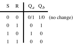
RS Latch
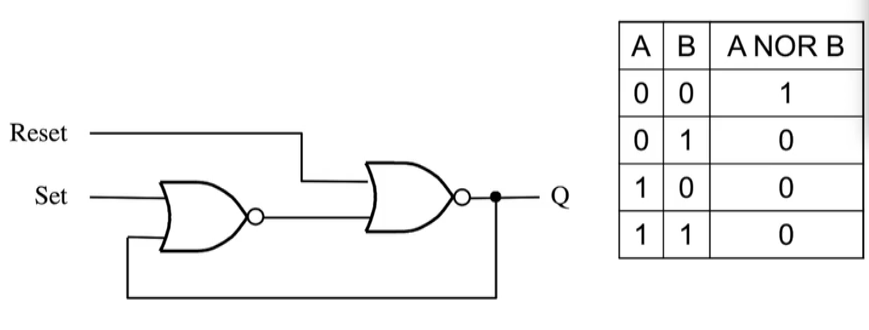
When SET is HIGH, the circuit maintains a HIGH output.
When RESET is HIGH, the circuit output maintains a LOW value.
Assumes that only one input is active at a time.
Undefined behaviour occurs when both inputs are HIGH
| Circuit | Table |
|---|---|
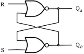 |  |
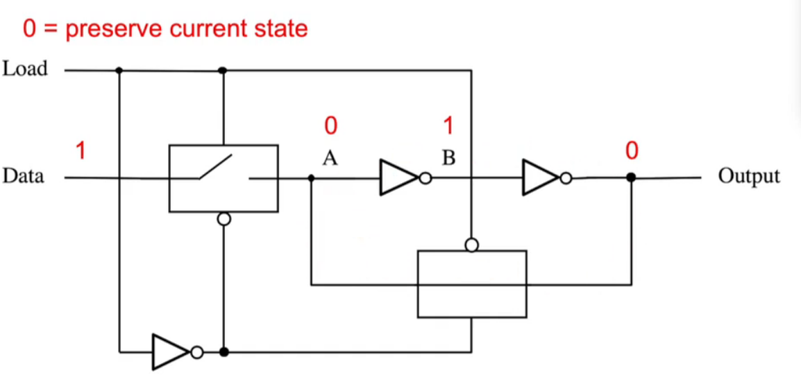
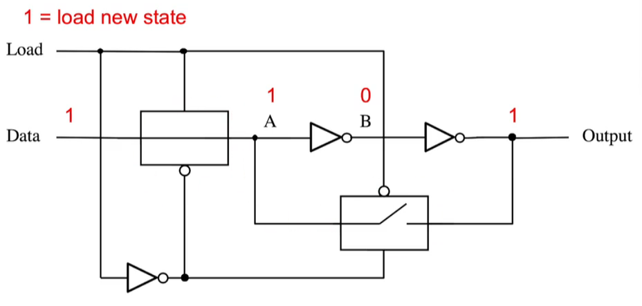
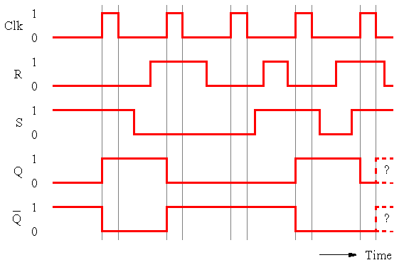
Clock-controlled RS Latch
A clock signal can be used to control when the latch will interact with different input states. When the clock signal is HIGH, the latch will respond.
This is done by implementing two AND gates - one for each NOR gate.
Note: The inputs are flipped
| Description | Circuit | Table | Symbol |
|---|---|---|---|
| Using AND and NOR | 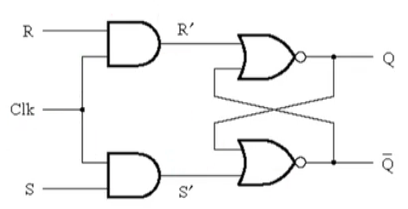 | 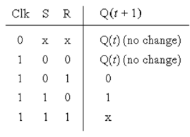 | 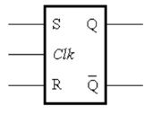 |
| Using NAND (better) | 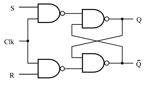 | 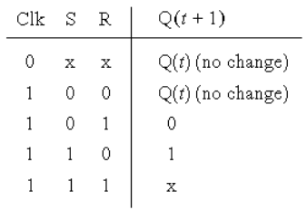 | |
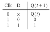
D Latch
Like the RS Latch, but has a defined behaviour for when $S = R = 1$.
The output follows the value of D when the clock is HIGH.
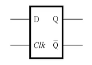
| Circuit | Table | Symbol |
|---|---|---|
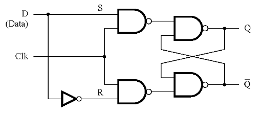 |  |  |
VHDL of a D latch
| |
Flip-Flop Circuits
Flip-flops are triggered on transitions of control signals
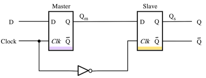
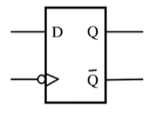
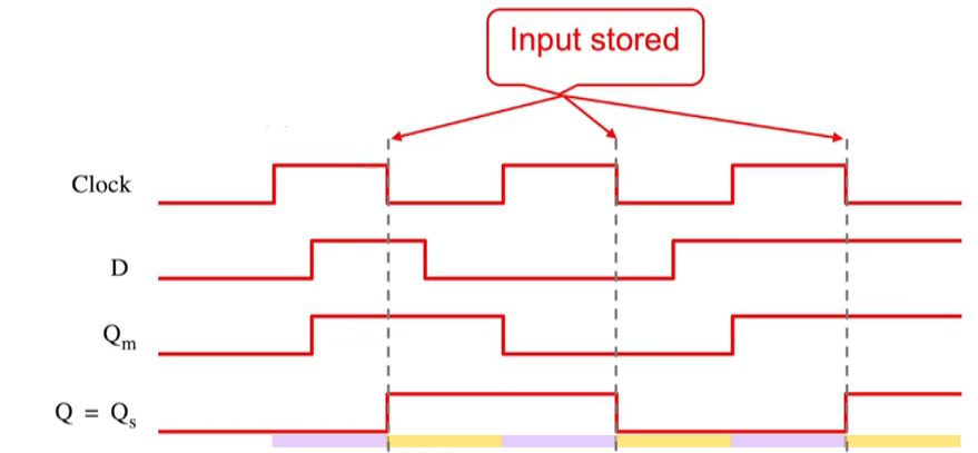
Negative-Edge Triggered (Master-Slave) D Flip-Flop
When the clock is HIGH, the MASTER latch is active.
When the clock is LOW, the SLAVE latch is active.
While the clock is LOW, as the MASTER latch is frozen (not active because its clock signal is LOW) - the output of $Q_m$ cannot change, hence the slave input will not change during the current clock cycle.
| Circuit | Symbol |
|---|---|
 |  |
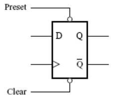
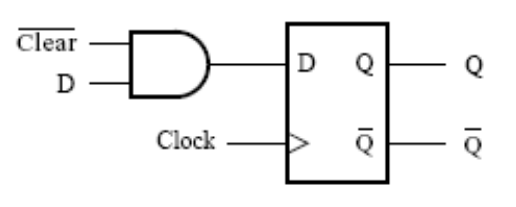
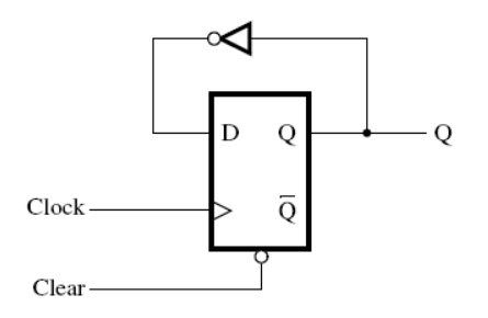
Preset and Clear triggers
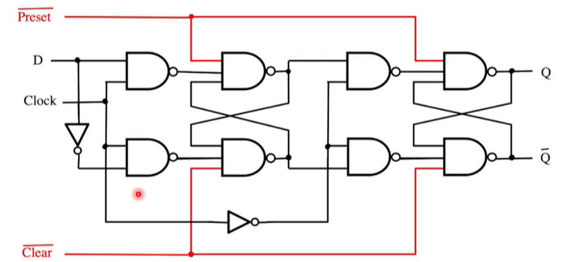
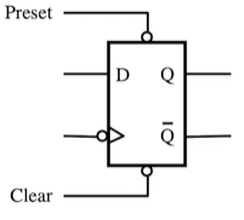
Pulling PRESET to LOW, forces the output Q to HIGH. Pulling CLEAR to LOW, forces the output Q to LOW.
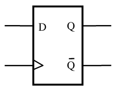
Positive-Edge Triggered (Master-Slave) D Flip-Flop
Whilst the clock inputs to the two latches could be inverted to form a positive-edge triggered D flip-flop, optimisations can be performed.
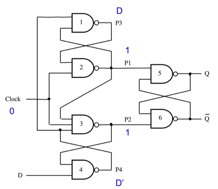
Note: If D -> 0 when the clock is HIGH, the output P2 prevents P4 from changing - hence maintaining a stable circuit.
This optimised circuit saves two NAND gates and one inverter gate.
Preset and Clear triggers
Asynchronous - doesn't care about the clock state
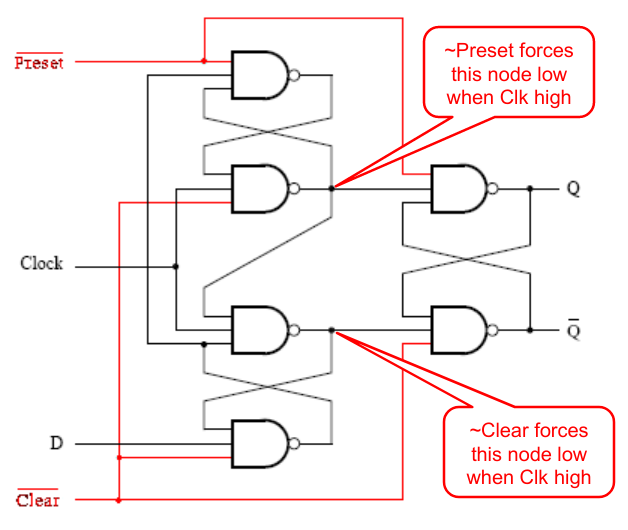
Synchronous - Only occur during active clock phase
VHDL for a Flip-Flop
Asynchronous
| |
With Reset
| |
Synchronous using WAIT UNTIL
| |
With Reset
| |
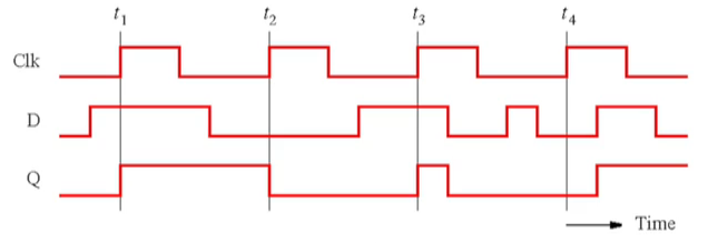
Comparison of D-type elements
| Circuit | Timing |
|---|---|
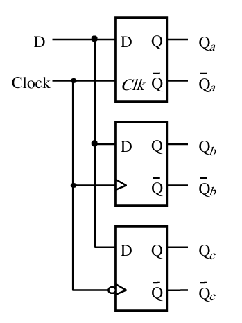 | 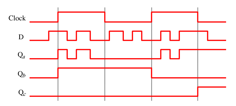 |
- D-latch ($Q_a$) - Follows the input of D while clock is HIGH
- Positive-edge triggered ($Q_b$) - Set to the initial value of D when the clock is HIGH
- Negative-edge triggered ($Q_c$) - Set to the initial value of D when the clock is LOW
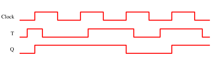
T-type Flip-Flops
"Toggle flip-flop"
When T is HIGH on an active clock edge, the value of Q is toggled.
| Circuit | Table | Symbol |
|---|---|---|
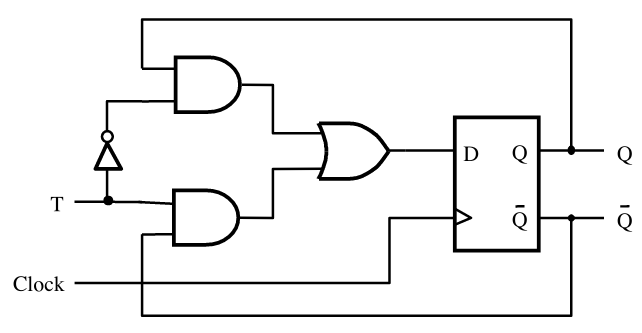 | 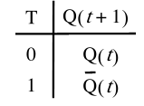 | 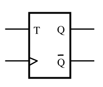 |
$Q(t+1) = T\ XOR\ Q(t)$
JK-Type Flip-Flop
| Circuit | Table | Symbol |
|---|---|---|
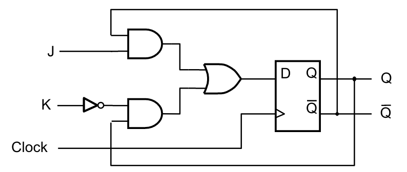 | 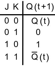 | 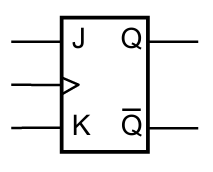 |
Electrical Timing of Flip-Flops
Propagation delay $t_{cQ}$
Time for the output to reflect an input change
The delay it takes to change from 1->0 may be different to the delay it takes to change from 0->1
e.g. Gated D-Latch
| 0->1 | 1->0 |
|---|---|
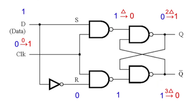 | 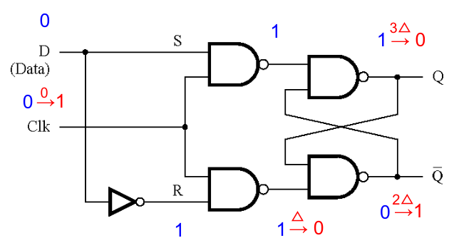 |
It takes $t_{cQ} = 2 \Delta$ for 0->1, but $t_{cQ} = 3 \Delta$ for 1->0.
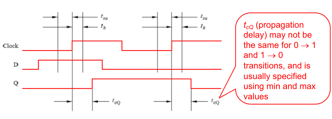
Setup time $t_{su}$ / Hold time $t_{h}$
Time the input needs to be stable for prior/after to the triggering edge (for reliable a read)
The circuit that generates the D signal must ensure the setup and hold times are satisfied. Together they define a window of time around the triggering clock edge for which D must be stable.
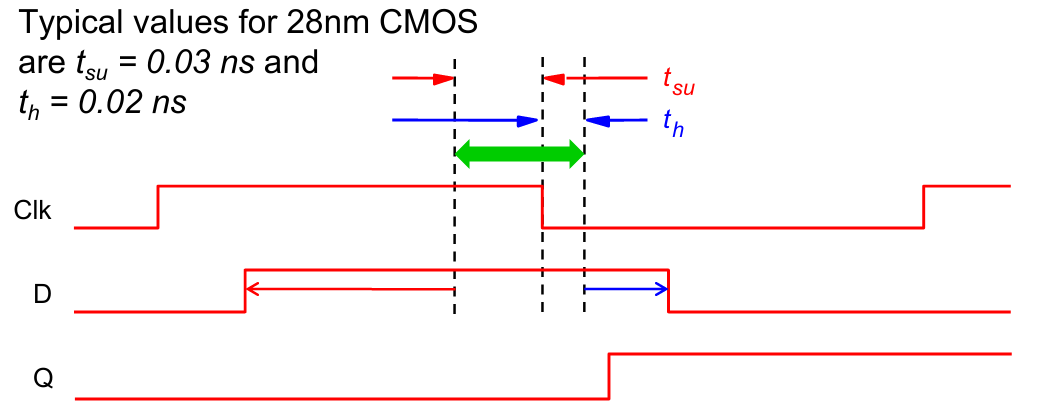
To determine minimum period $T_{min}$ to wait for a guaranteed success (i.e. critical path - which is the longest delay).
$$ T_{min} = \frac{1}{F_{max}} $$
$$ T_{min}$ = max(t_{cQ}) + t_{NOT} + t_{su} $$ $$ F_{max} = \frac{1}{T_{min}} $$
Therefore, max clock speed is $ F_{max} $ Any faster, $t_{su}$ will not be satisfied
To determine the shortest delay from any positive clock edge to flip-flop input.
$$ min(t_{cQ}) + t_{NOT} > t_h $$
Clock Skew
Delay of the arrival clock edges, as a result of wire delays.
FPGAs have special clock distribution networks designed so that all components receive the clock at the same time.
Positive Clock Skew can be beneficial, as signals may arrive earlier than expected at the next gate.
Negative Clock Skew is often harmful, as the signal arrives later than expected, adding further delay to the circuit.