Single Cycle Processors
Contents
Steps to Build a Processor
Analyse instruction set to determine datapath requirements
Select a set of hardware components for the datapath and establish clocking methodology
Assemble datapath to meet the requirements
Analyse implementation of each instruction to determine control points
Assemble the control logic
Analyse instruction set to determine datapath requirements
The requirements of each register can be identified as a set of register transfer operations. Data transferred from one storage location to another may go through a combinational logic to occur.
Register-level Transfer Language (RTL) is used to describe the instruction execution.
e.g. $3 <- $1 + $2 for ADDU $3, $1, $2
The datapath must support each transfer operation
All instructions start by first fetching the instruction from memory.
In MIPS-Lite, all instructions are either
op | rs | rt | rd | shamt | functorop | rs | rt | imm16
Some of these instructions (e.g) do the following register transfers:
To support these, the instruction set must have some sort of memory (instruction and data), program counter (PC), registers (to read/write
rs/rt/rd), add/sub/or operations for registers or extended immediate values, and to increase the program counter
Select a set of components for the datapath and establish clocking methodology
Combinational Elements
Adders, Muxers, ALU
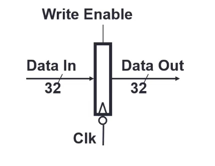
Storage Elements
Registers
A set of flip-flop components.
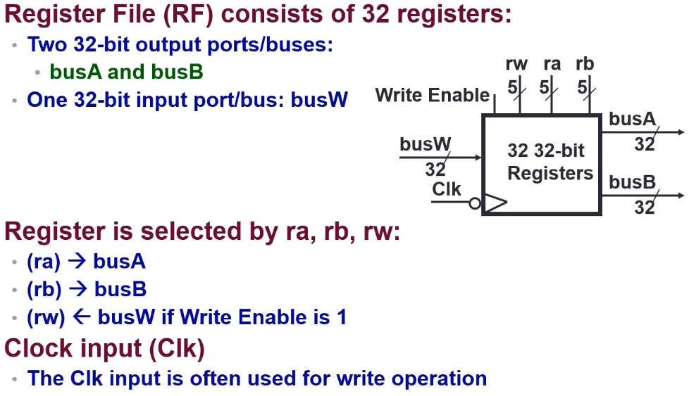
Register File
A set of registers
Memory
- One input port/bus for data in
- One output port/bus for data out
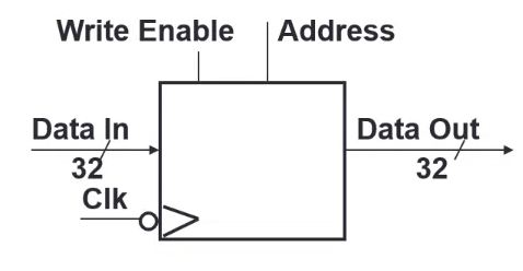
The memory word is selected by the address.
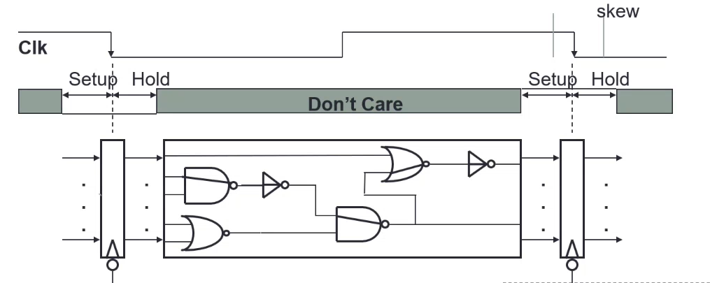
Clocking Methodology
Edge triggered clocking - all storage elements are clocked by the same clocked edge
Need to consider the following issues
- Clock skew - difference in the arrival of the clock signal
- Setup time - period of stable input for the register to read successfully
- Hold time - period of stable output for the register output
-
- Cycle time >=
Clk-to-Q+ longest delay path + setup + clock skew Clk-to-Q+ shortest delay path - clock skew > hold time
(Clk-to-Q - The delay of the register)
Assemble datapath to meet the requirements
Put the selected components together based on the register transfer requirements
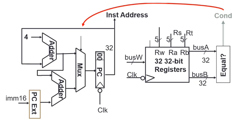
At the start of each clock cycle, fetch the instruction from MEM[PC].
At the end of the cycle, update the program counter.
Either PC <- PC + 4 or PC <- ... (branch)
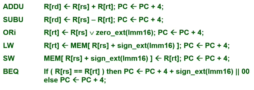
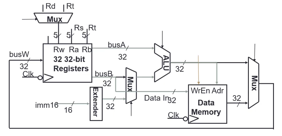
ADDU / SUBU
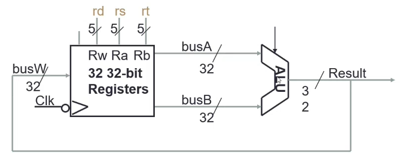
ORI
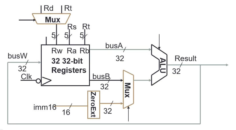
The second input to the ALU is switched by a multiplexer between BUS B and a 16-bit immediate value (zero extended to 32 bits). Rw is also switched by a multiplexer
LW
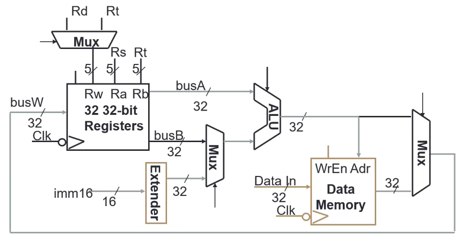
SW
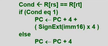
BEG
Analyse implementation of each instruction to determine control points
Instructions are encoded using binary code.
In a single cycle datapath, each instruction must be completed in one clock cycle.
Find the control signals (i.e. signal to the multiplexer)
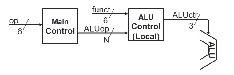
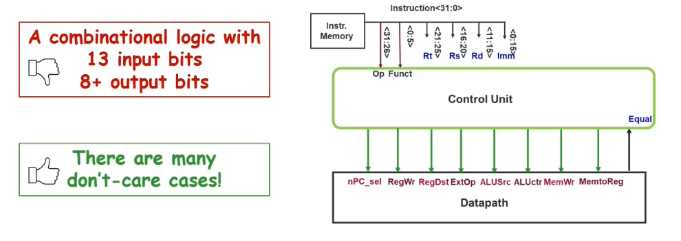
Assemble the control logic
A control unit takes in the instruction (op, funct) and datapath eq, to output control signals on the control datapaths.
i.e.
Multi-level Control Logic
A single level of control logic may be costly (have to factor in many cases). Instead it may be beneficial to have a second stage/level of instruction control handling.
Local decoding of instruction categories can make the design smaller, simpler and faster.
e.g a control unit that only handles ALU controls