Multi Cycle Processors
Contents
The clock cycle speed is originally limited by the longest instruction time. In multi-cycle processors, instructions are split into several cycles, therefore the clock cycle time can be reduced. Each instruction is laid out to use the smallest number of clock cycles possible
For a small set of instructions, it is relatively simple to design a single-cycle processor to implement the functionality for the instructions..
We may want to assume that control signals will be ready when data flows to a component
With a CPI = 1 processor, the clock cycle time is determined by the latency of the longest instruction - which means that all instructions take as much time as the slowest instruction.
In addition, we need to duplicate resources that are used more than once per instruction.
To improve this design, we can allow instructions to span over multiple cycles.
In a way, we are able to 'quantize' the steps of the instruction.
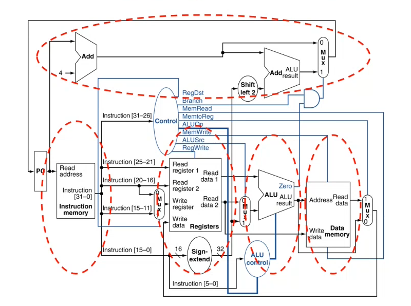
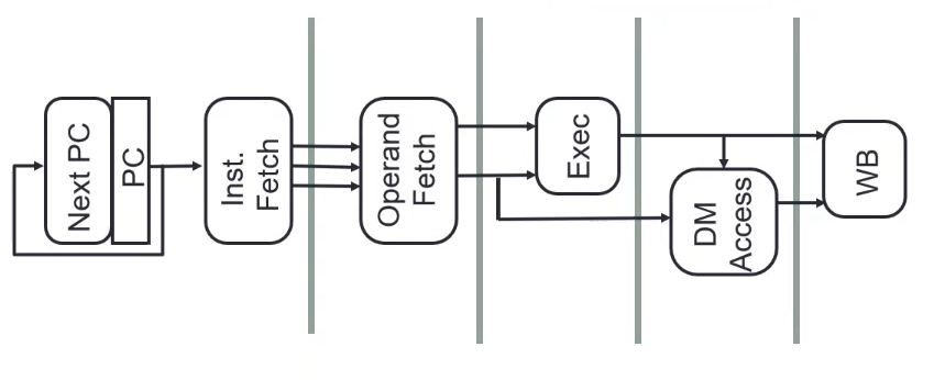
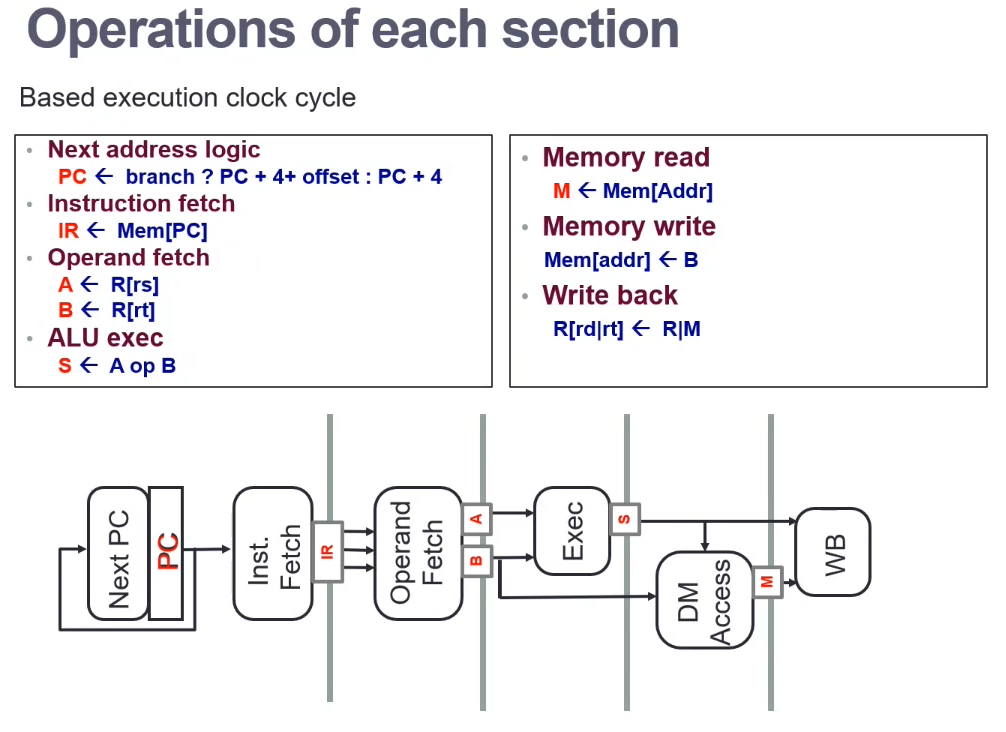
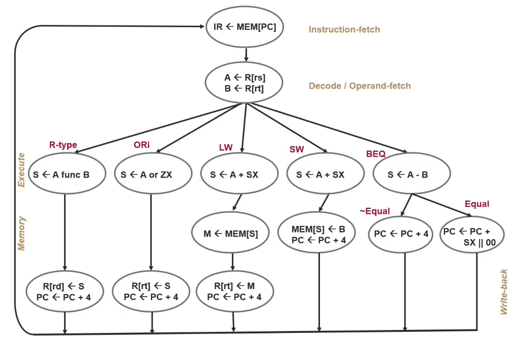
This multi-cycle processor design can be implemented by partitioning the single-cycle datapath, where each section takes one clock cycle to execute. By repeating parts of the cycle, we also mitigate the need to duplicate resources
The time spent in each section should be balanced, as the clock cycle time is determined by the longest section delay. Registers should be inserted between sections, based on the operation of each section
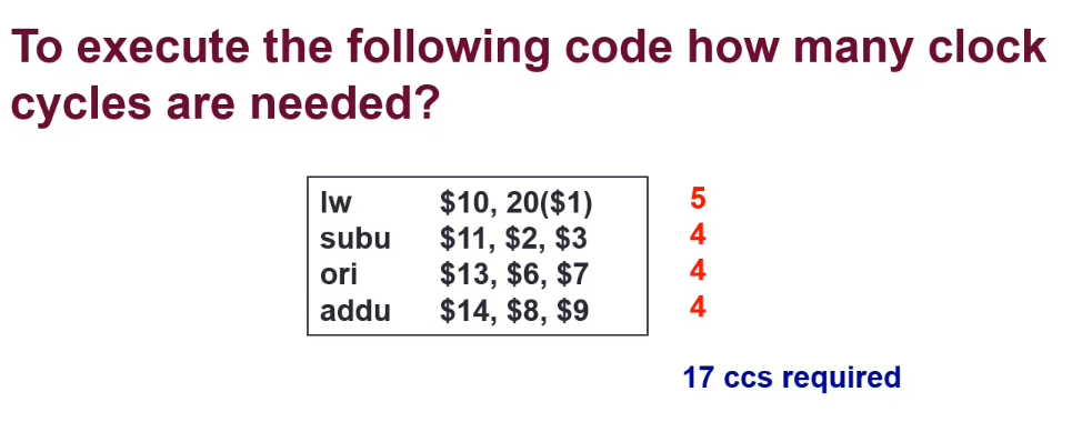
Most instructions take up 4 cycles
R-Type Instructions - Takes 4 cycles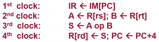
I-Type Instructions - Takes 4 cycles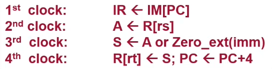
LW Instruction - Takes 5 cycles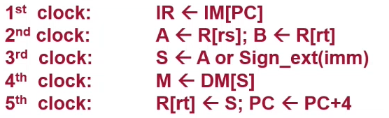
SW Instruction - Takes 4 cycles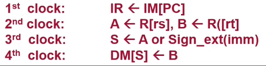
BEQ Instruction - Takes 4 cycles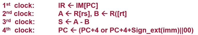
Building Finite State Machines for Control
As instructions are no longer single-cycled, we can no longer use combinational logic to determine the control signals. Instead we need to use a FSM (and deal with it in steps).
(Each horizontal level related to one clock cycle)
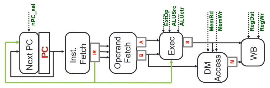
nPC_sel, ALUSrc, ALUctr, ExtOp is needed for BEQ instruction.