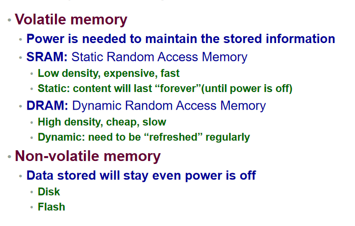
Introduction to Memory
Contents
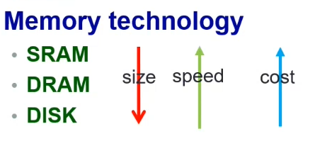
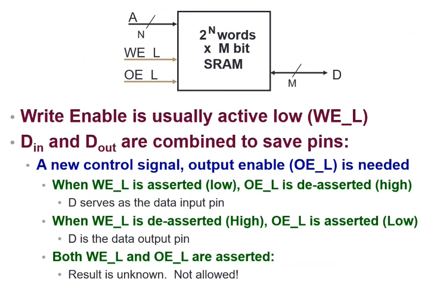
SRAM (Volatile)
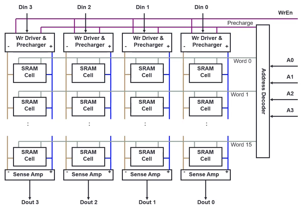
16-word 4-bit SRAM structure
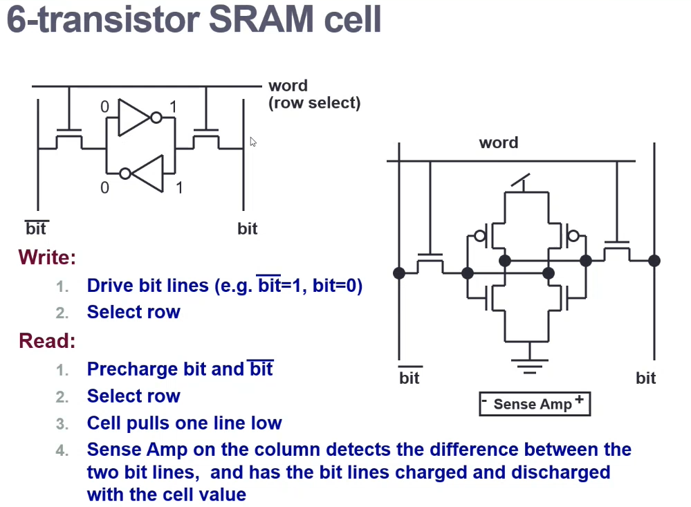
- Precharge required to get the electrical components to their required voltage/energy
DRAM (Volatile)
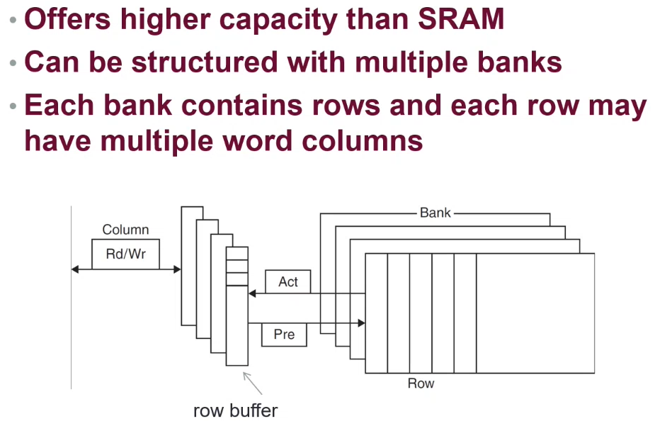
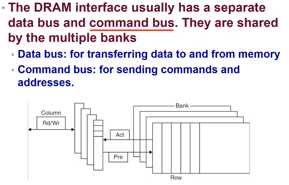
Typical DRAM bank
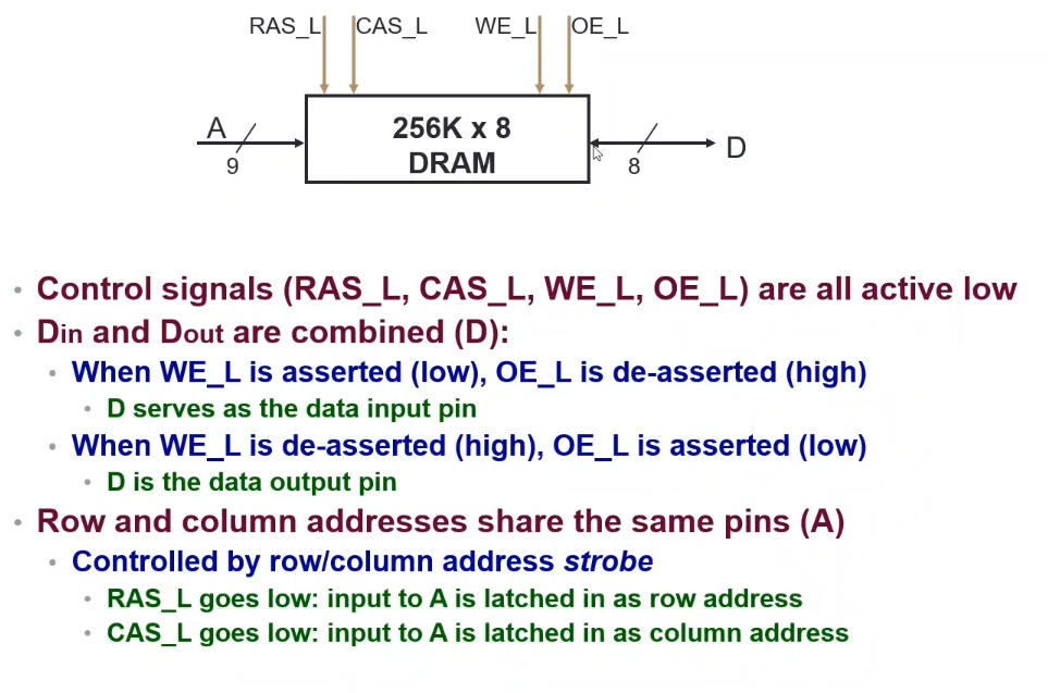
Only half the number of address bits is required, as we can switch usage of the input as a row or column selector
1-transistor DRAM cell
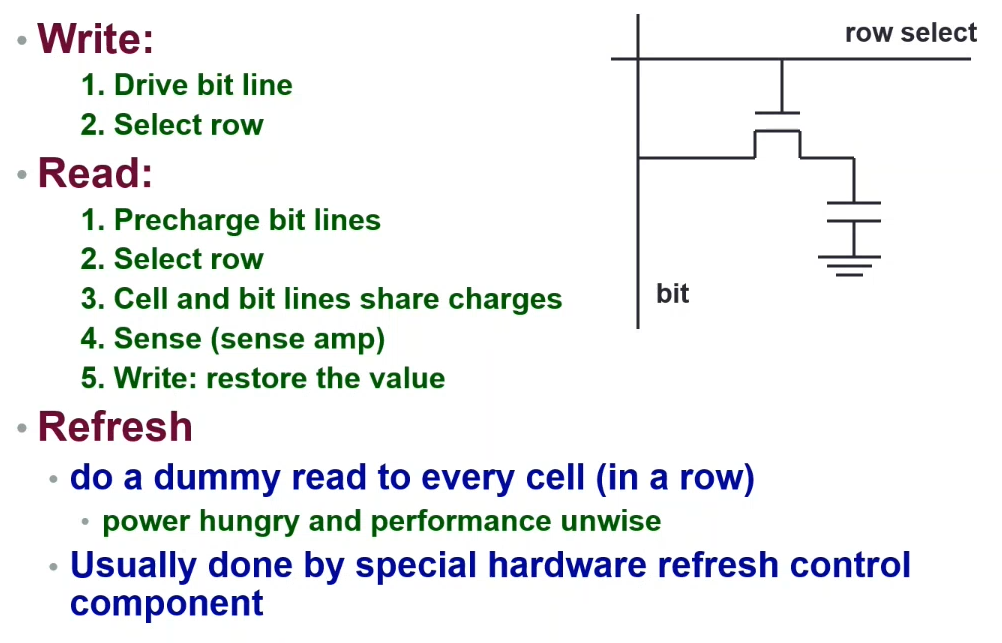
As a result of the circuit configuration, the voltage/current in the capacitor can drain over time. Therefore a refresh is required (i.e. doing a dummy read/write to every cell in a row) - which is often performed by special hardware refresh control components. This operation is power hungry and sacrifices performance.
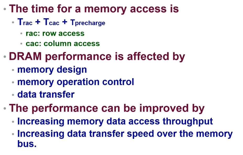
DRAM Access Cycle
The entire row must be read at a time
- Open the row related to the memory location (and precharge)
- Access the column (read / write)
- Precharge the bit lines for the next different row access
Performance
Increasing Data Throughput
Burst Mode - Consecutive accesses without the need to send the address of each word in the row.
Saves T_rac (row access delay), by only sending the other required column (word) addressess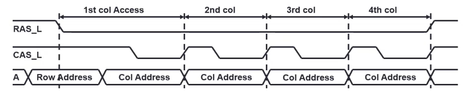
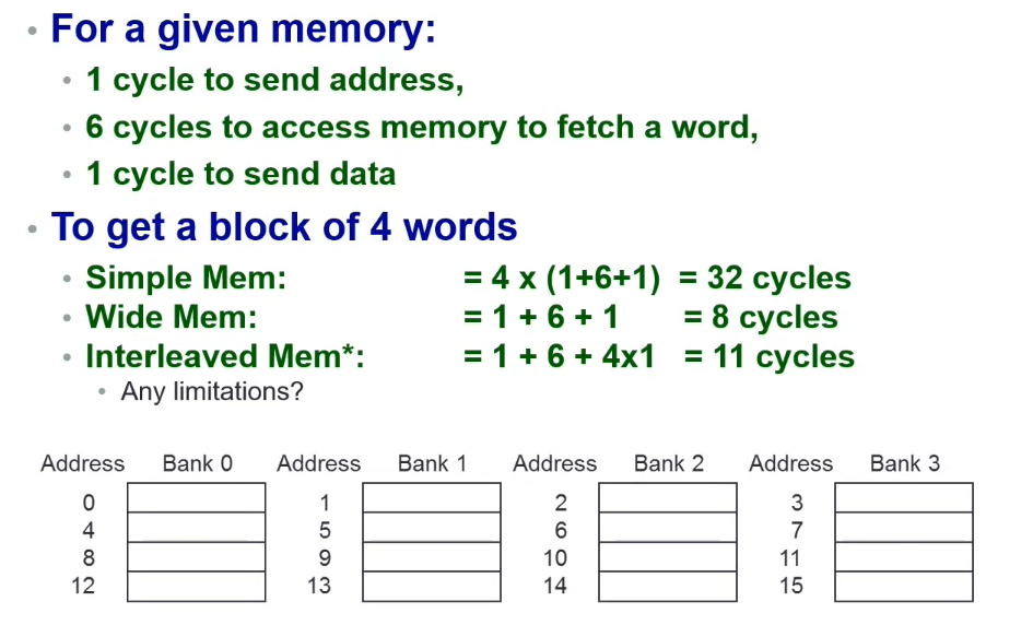
Multi-bank Interleaved Access - Access different banks at the same time.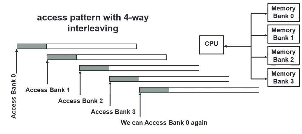
Wide memory data bus - Transfer multiple words at the same time along the data bus line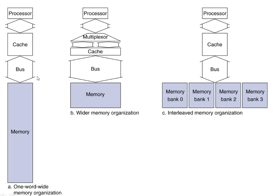
Increasing Data Rate
DDR DRAM (Double Data Rate) - Transfer on both rising and falling clock edges
QDR DRAM (Quad Data Rate) - DDR functionality on separate input and output port
Hard Disk Drives (HDD) - Non-Volatile
Disks contains magnetically-coated platters, which contain tracks that are split into sectors.
The magnetic orientation of the field represents a bit.
The controller handles the read/write mechanism, motor operation, etc.
Performance / Delays
- Seek time - time between file request and when the first byte is received (~10-20ms)
- Rotational latency - time required for the first bit of the data sector to pass through the read/write head (~2-4ms)
- Data rate - bytes per second that the drive can deliver to the CPU
Solid State Disks (SSD) and Flash
- Everything is electronic - no mechanical moving parts
- Each cell is a modified transistor with a floating gate and a control gate
- The two gates are separated by a thin oxide layer
- The floating gate 'links' to the word line throug the control gate with a small threshold
- When linked, the cell has a value of
1, else0 - When unlinked (through negative electrons acting as a barrier), there is a large threshold; preventing current from flowing
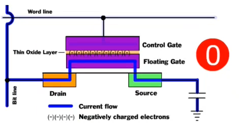

- When linked, the cell has a value of
Trends | CPU vs Memory improvements
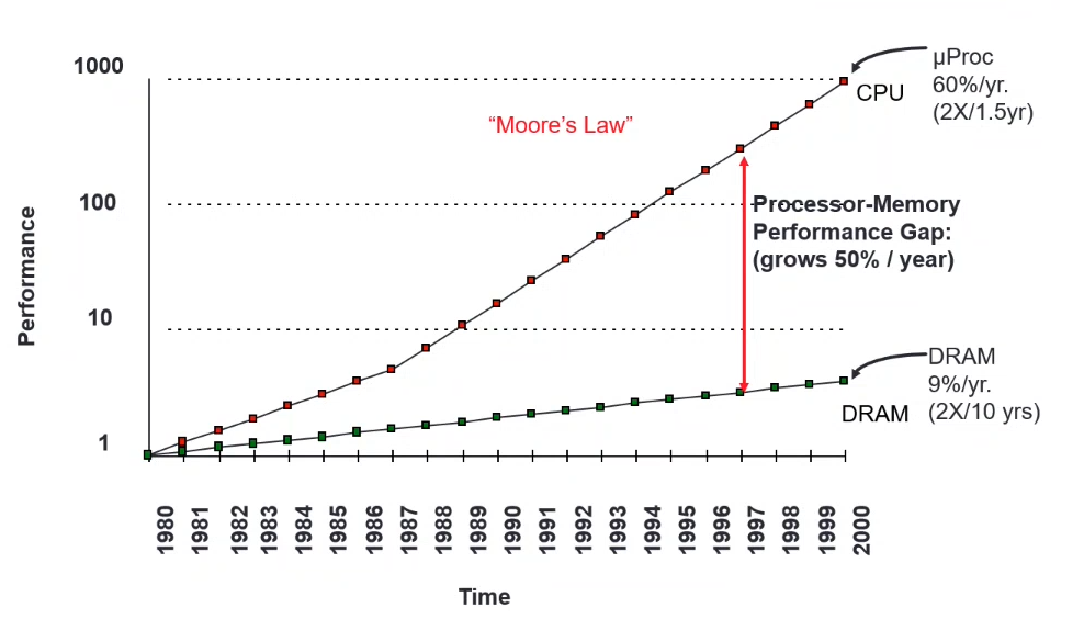
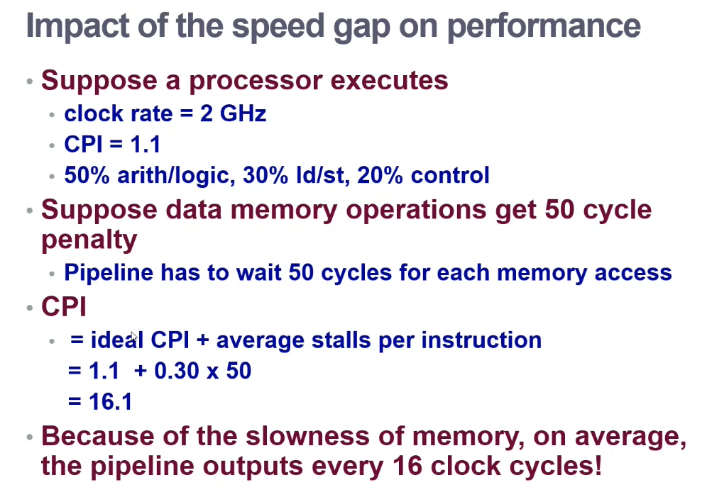
Slow memory affects speed by quite a lot!
Memory Hierarchy
Changing the external representation of memory so that it appears, fast, cheap and large.
- Store everything on the disk
- Copy recent required data from the disk to the smaller DRAM ("main memory")
- Copy more recently accessed and nearby items from the DRAM to an even smaller SRAM ("cache")
Typical two-level memory hierarchy
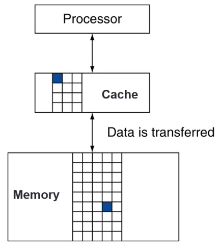
The processor accesses cache for data
Cache Hit - The accessed data is present in the cache
Cache Miss - The required data is not in the cache; copy the data from the memory to the cache
- Cache Hit Rate =
Hits / Accesses - Hit Time - Time taken to access the cache
- Cache Miss Rate =
Misses / Accesses=1 - hit rate - Miss Penalty - The time taken to copy the data block from the memory to the cache
Principle Of Locality
Programs tends to access a relatively small portion of the address space over a small period of time.
- Temporal Locality (Time) - Will tend to be referenced again
- i.e. leave items in the cache
- Spatial Locality (Space) - Nearby addresses will likely to be accessed
- i.e. move a bunch of data to the cache
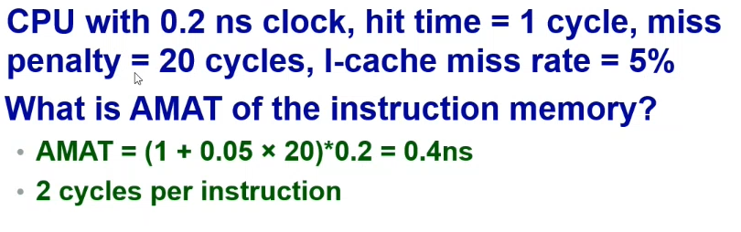
Average Access Time
Average memory access time (AMAT) = Hit time + Miss rate * Miss penalty
- Register <-> Memory operation is implemented by the compiler / programmer
- Cache <-> Memory operation is implemented by hardware
- Memory <-> Disk operation is implemented by the hardware, OS (virtual memory), and the programmer