Lab 2
Contents
Task 1
Implementation Overview
| Original | SLL | BNE |
|---|---|---|
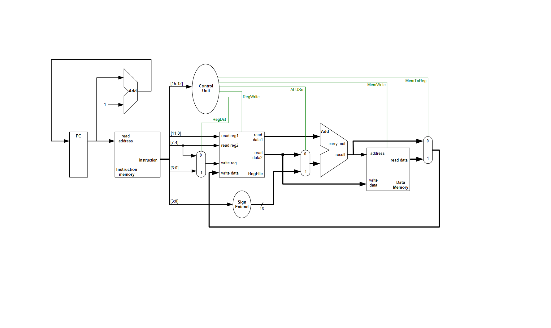 | 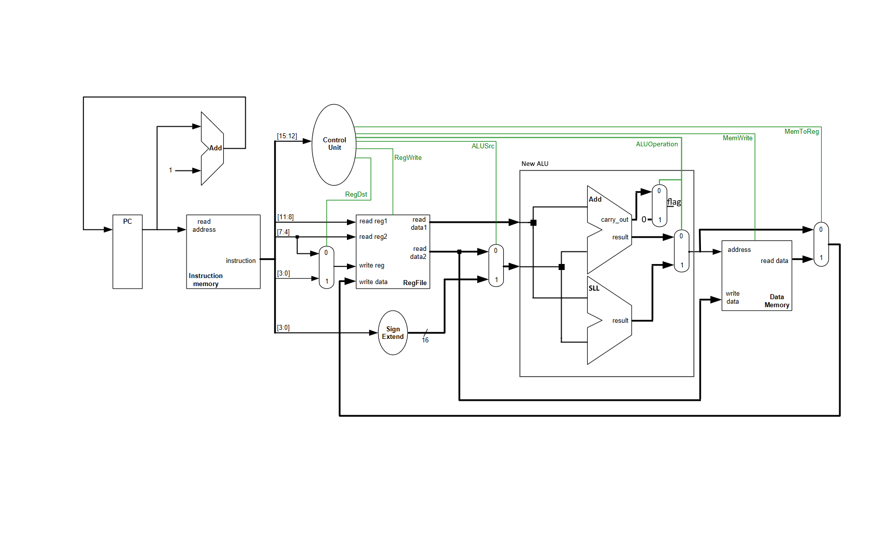 | 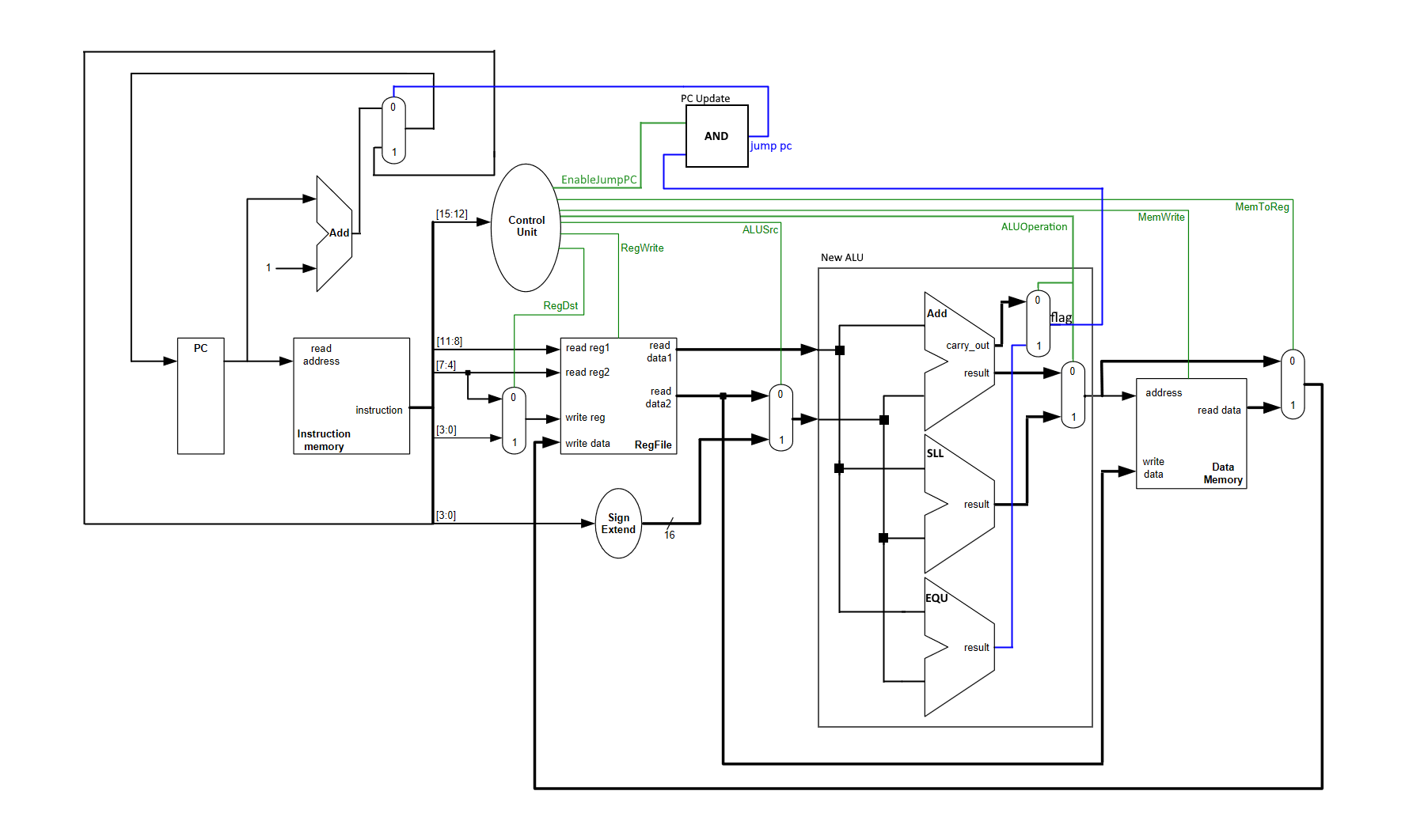 |
- Added a bit-shifter and comparator into the ALU. The ALU switches the result and miscellaneous flag bit depending on an introduced ALUOperation control signal.
- Added a multiplexer that switches between the next "standard" PC address, and the 4-bit address in the instruction, controlled by an introduced EnableJumpPC control signal that is AND gated with the ALU output flag
- Highly opinionated design (i.e. ALU flag defaults to comparator output for all instructions except for ADD)
Introduced Instructions
| |
Introduced Control Signals
| |
Step 0 (Original)
Implement SLL
Implement BNE
Simulation
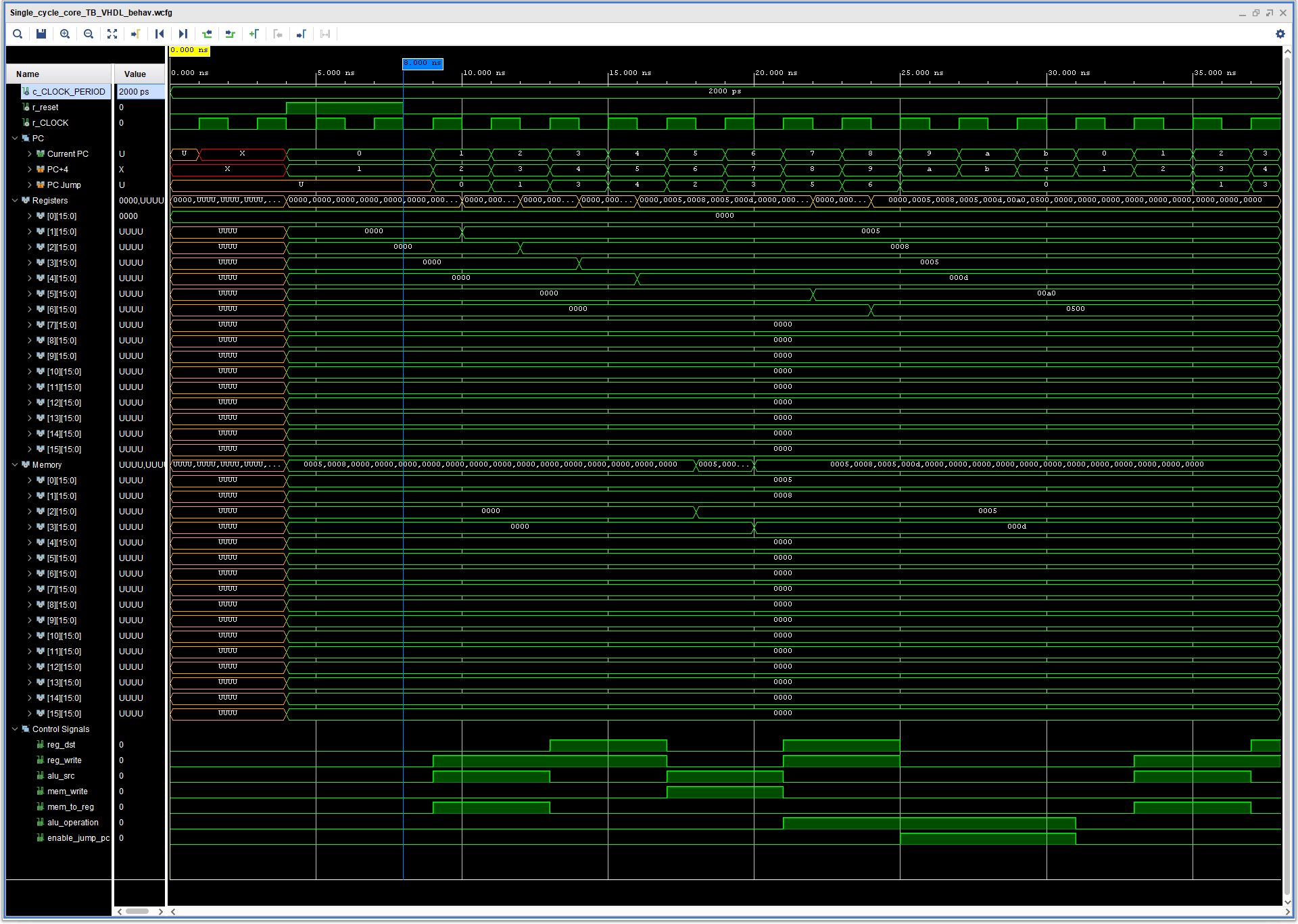
| |
Task 2
Hi Kenny / Brian :)
I don't have time to actually implement and test it, but I reckon explaining what I would do to the design would suffice some marks :)
This design incorporates a stack entity that co-exists with the RegFile since the task spec said to port ALL of the operations - inclusive of the write and store operations.
Stack Management
- We could create an entity that internally keeps track of its stack pointer (
INTEGER RANGE 0 TO 15). - When the
enablebit is asserted anddirectionis set to0(for POP), the 16-bitvaluebus is set to the internal stack memory array at position SP, and SP is increased by 1 (towards the bottom of the stack,15). - When the
enablebit is asserted anddirectionis set to1(for PUSH), the internal stack memory at position SP is set to thevaluebus, and SP is decreased by 1 - When the
resetbit is asserted, the stack will be reset
Design Choices
- When resetting the stack, the data will not be cleared; only the pointer will be reset
- No protections against stack overflows/underflows will be implemented
- Stack direction: 15 (bottom) -> 0 (top)
Considerations
In the previous single cycle core design, the value of two registers were read simultaneously. While unconventional, the stack design could return the value at SP, as well as SP+1 (value before the top) - which would allow for two values to be read during the same cycle
For the writeback (i.e. a push instruction, or the result of add / sll / etc), this can occur during the falling edge of the clock signal, similar to the other memory entities.
Instructions
By migrating to stack-based operation, the instructions no longer need their rs and rd fields (with the exception of pop $rd) - which allows the ISA set to have 8-bit wide instructions instead of 16-bits
ISA (8-bit wide)
noopadd- pop, pop, exec, pushsll [imm]- pop, exec, pushbne [imm]- pop, pop, execload [imm]- pop, execstore [imm]- pop, execpush [imm]- pushpop [reg]- pop
ISA (Multi-width instructions)
- (4)
noop - (4)
add- pop, pop, exec, push - (4)
sll- pop, pop, exec, push - (4)
bne- pop, pop, pop, exec - (4)
load- pop, pop, exec - (4)
store- pop, pop, exec - (8)
push [imm]- push - (8)
pop [reg]- pop
When using multi-width instructions, the opcodes should be specifically crafted in a way that allows the control unit to know to advance 4 or 8 bytes for the next instruction. In our case where we have 8 instructions, the opcodes for all the 4-bit wide instructions can all start with 0; and the opcodes for the two 8-bit wide instructions can both start with 1
When implementing this reduced width instruction set, all references to 16-bit instructions (15 downto 0) can be changed to 7 downto 0. As registers still exist within the system, the stack entity should be placed between the instruction memory and the RegFile entity. This way, if the load or store operations are executed, the stack can retrieve the register addresses from the stack - which can then be passed into the RegFile.
The writeback stage also needs to be modified to push the result to the stack, rather than to the RegFile. For reasons aforementioned, a mux should be used to route the result either to the stack, or to the RegFile for load and store operations.
For the bne instruction, if the 4-bit wide variant is used; the jump address should always be popped off the stack, regardless if the processor will perform the jump or not. For the 8-bit wide variant, this is not an issue. In addition, the implementation of the 8-bit wide variant will be simpler as the address in the instruction can be routed directly into the PC mux. (Tradeoffs between instruction size, operation speed, and circuit complexity, yada yada..)